The sine bridge section is a specific implementation of direct digital synthesis (DDS). Theory first, then some details on the unit.
A sine wave, or any time varying signal, can be represented by a set of discrete voltages representing the signal's amplitude at specific points in time. The more discrete voltages representing the signal over a given time interval, the higher the resolution.
At its core this is what the sine bridge does. It uses a controller (MCU) with a fixed table representing the sine wave's amplitude at specific time points. The controller 'plays' each of these values at a fixed frequency through an LC filter to obtain a fairly distortion free sine wave.
The sine bridge achieves this through the use of a full [H] bridge and LC filter like that used in a flyback power supply. In fact, some of its design & operation is very similar to a flyback.
The controller contains a table with one hundred values. Each of these represents the voltage of the sine wave at a particular angle. It was previously mentioned that the values are related to time, which in this case is equivalent to angle because the unit is producing a sine wave at a single frequency.
The MCU accomplishes this by the frequency used to 'play back' the values. The frequency must be evenly divisible into the fundamental (output) frequency or it will be off and contain harmonics.
It was also previously mentioned that the sine unit functions similar to a flyback converter. More specifically, it functions like a flyback converter with the output inductor operating in continuous mode (this makes the math a bit easier). Neglecting losses, the output voltage of a flyback operating in continuous mode is determined by the formula Vin * D = Vout where D represents the on-time, or duty cycle, of the PWM period. So the table of values contained in the MCU are actually the on-times with which to vary a PWM's duty cycle.
Bringing it all together. The MCU uses a PWM to drive a full bridge at 24kHz. At this frequency, exactly 400 periods will occur in the time required for a single 60Hz cycle (16.666667mS). The MCU's table contains one hundred entries representing on-time (D) values for sine angles between 0 and 90 degrees. Starting a 0, the MCU loads the first value to the PWM and starts the bridge. During that period the second value in the table is loaded (it latches to the PWM at the start of next cycle).
This process repeats until the end of the table is reached - 90 degrees. The MCU then repeats the process in reverse, counting down from 90 - 0. At this point half of a sine wave has been produced. To complete the remaining half the MCU reverses the bridge direction and repeats the entire process. Again at 360 degrees the MCU reverses the bridge and continues.
Throughout this process the output of the bridge passes through LC filter to perform the voltage averaging function and presents a clean 60Hz sine wave.
The PWM and bridge control are mostly handled in the MCU's hardware but, the loading of the table is handled in firmware and is time critical. For this reason it's handled by a non-maskable interrupt handler. This, along with some other characteristics of MCUs, presents considerations & limitations for this approach:
- Sine wave resolution is dictated by table size which in turn is dictated by the MCU's processor speed. The MCU must have sufficient execution margin to load the table and still perform other tasks (temperature monitoring, communication, etc.).
- The table size should meet the Nyquist criteria. The TS50 violates it (should be 200) but with a single frequency/waveform the LC filter masks most of it.
- Even with the correct frequency set to drive the PWM there will be harmonics in the output. This is because of the inherent drift & jitter present in the on-board clock oscillators of most MCUs. Practically speaking this isn't a big deal unless your building a grid-tied inverter or are powering devices that derive timekeeping from the AC line. The oscillator's tolerance translates to +/- 1Hz of drift.
- A larger table results in a smaller output inductor (more on this later).
All of these can be overcome in the design without extraordinary effort. The TS50's sine module uses an 8-bit MCU running at a 6MHz instruction speed. The workbook attached to this project contains the model and table values for the TS50. The pwmtable tab contains the calculations for each table entry along with a graph. Very instructive to see how changing values effects the signal.
Implementation details. Electrically a bit more is happening. The full bridge doesn't quite function like a conventional one. It has two distinct modes of operation: charge and flyback, and each occur during a period (cycle).

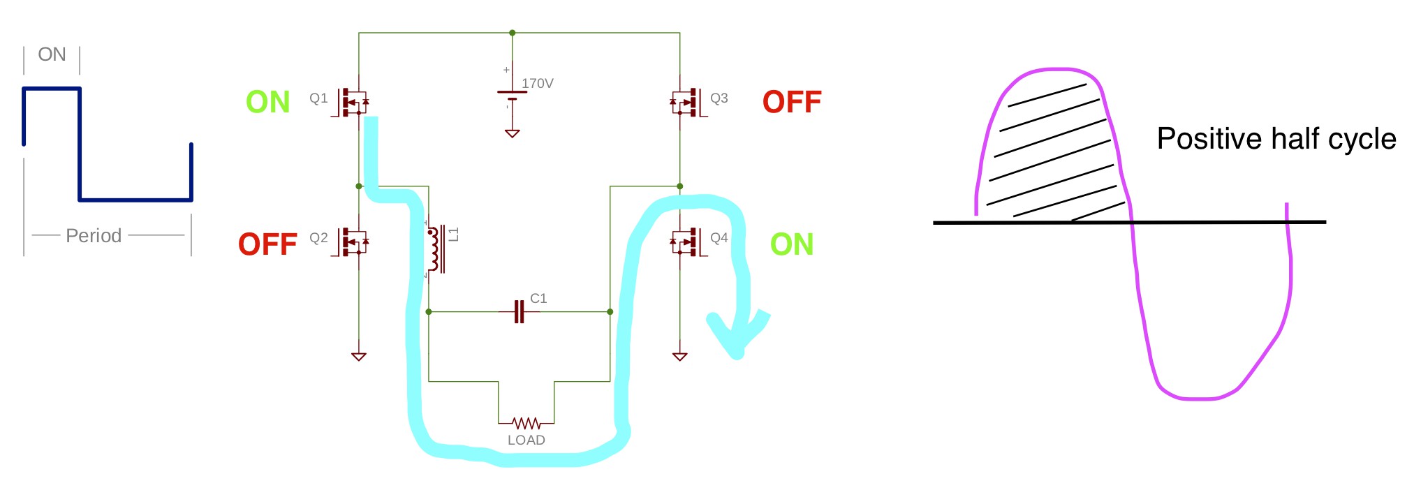
Charge mode occurs during the PWM on-time, or D, and is like that of a conventional bridge. Current flows through the high-side MOSFET, from the HV supply, through the output inductor & load, and finally through the opposing low-side MOSFET returning to the supply. This mode is referred to as charging because, like a flyback, the inductor is also charging (storing energy in its core).

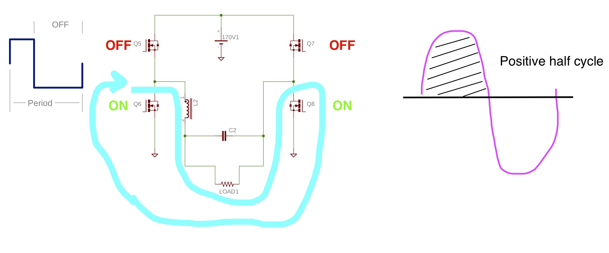
Flyback mode occurs when the PWM's duty cycle is complete. The high-side switch is now off but the opposing low-side remains on. Additionally, the same-side low turns on to support the flyback action of the inductor. The inductor, having reversed polarity, maintains the flow of current in a loop through the load, through the low-side MOSFETS & ground plane, and back to the inductor.
This process will repeat each period through 180 degrees of sine and then repeat with the MCU maintaining the opposite low-side switch on for the duration. Current flow & switch is opposite the diagrams but electrically the operation is identical. This control is implemented in the MCU through a combination of peripherals and firmware.
The remainder of the sine module's design is unremarkable with the exception of the output inductor (L1). A good starting point is to design as a continuous buck. Calculate the required inductance first:
L = (Vout * T * (1 - Dmin)) / (2 * Iomin)
- L = inductance
- Vout = maximum output voltage, 170V for 120 VAC RMS
- T = bridge period in seconds (41.66uS for 24kHz)
- Dmin = minimum duty cycle in %
- Iomin = minimum output current
You can get some crazy numbers depending on what you plug in for Dmin and Iomin. Dmin is changing every period and putting in 0 (which the 1st few cycles in the pattern will be) will over-size the inductor. 0.05 (5%) is a good place to start.
Iomin actually represents the critical inductor current, or the current below which the inductor becomes discontinuous (i.e. completely discharged). This is the parameter to pay the most attention to and assuming T & Vout are fixed, will most affect the design. It's suggested to start with Iomin at the mid-point of the design's current rating (e.g. for an inverter rated at 1A RMS start with 0.5).
A word of caution: don't think that bigger is better. A large inductance value will require a large core with a large number of turns and high dissipation. If the value is too high it will distort the sine wave (cut-off frequency is too low).
This can be easily seen if the approach to the inductor's design is that of a second order (2-pole) filter: (ζ / ω) * 2 * R where R is the load in ohms. As load increase (R decreases) the required inductance goes down.
Once the inductance is established the core type & material can be selected and the design completed for wire selection & turns, temperature rise, core, and copper losses.
With L1 established the value for C1 can be calculated: 1 / (L * ω^2). Values should be in the 1 - 6 uF range. Be sure to select one with suitable margin for voltage ratings. The capacitor will see the full DC voltage of the bridge along with the AC component.
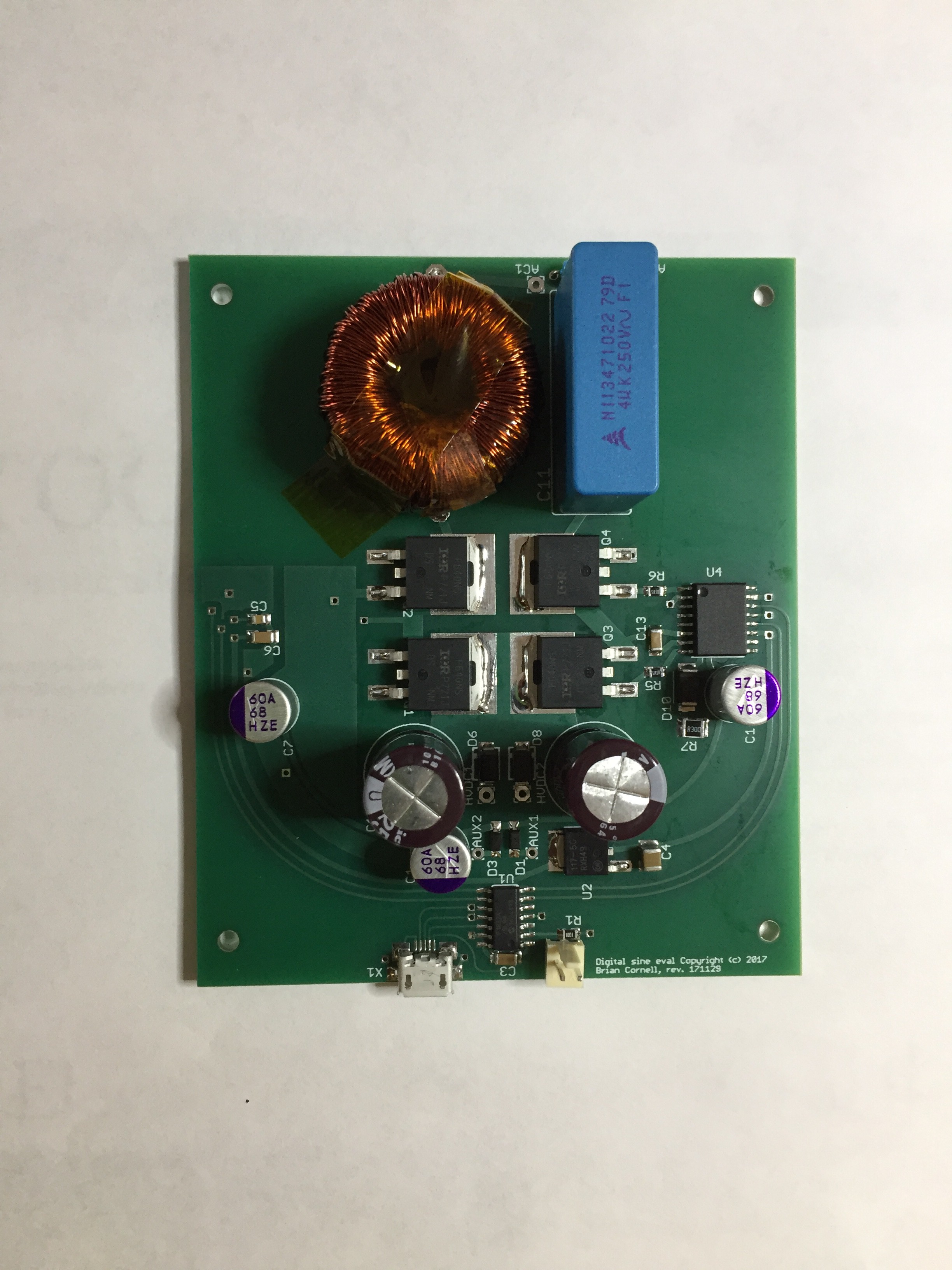
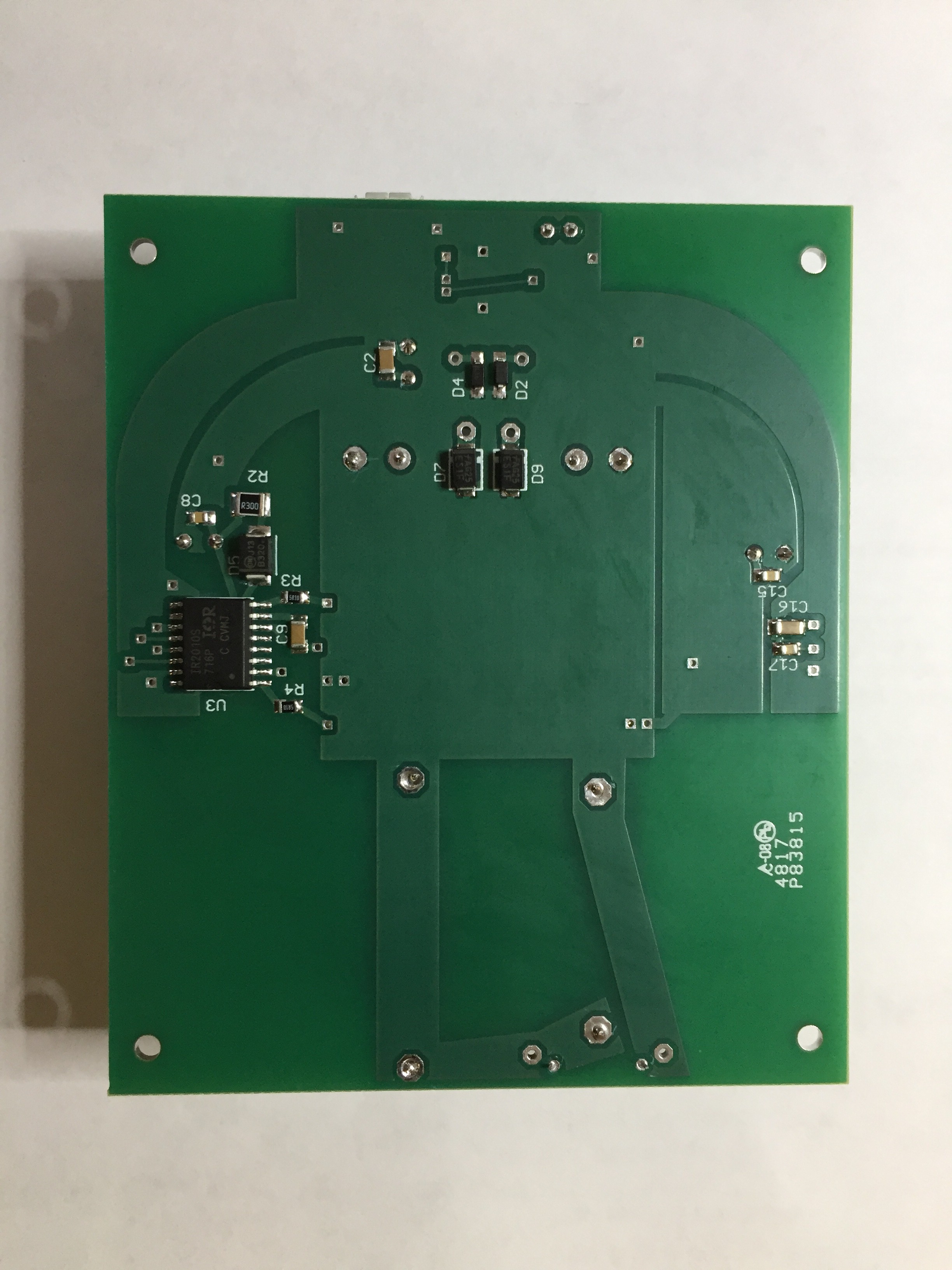
Below are pics of the top & bottom of the sine module as implemented in the TS50. The one modification was to grind off the 'leg' traces on the bottom of the board: that was a layout error and resulted in a current loop generating EMI.


Discussions
Become a Hackaday.io Member
Create an account to leave a comment. Already have an account? Log In.