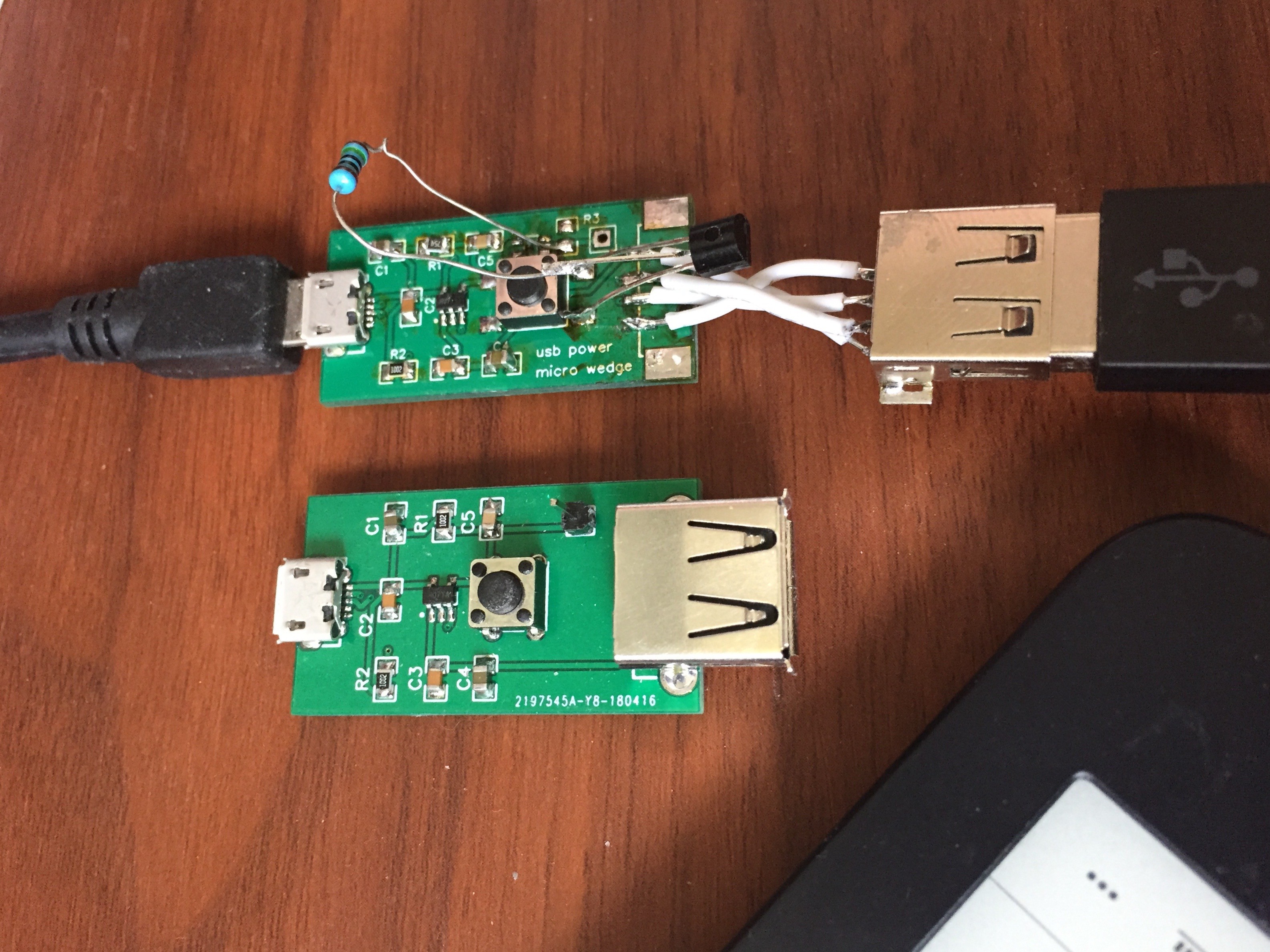
One other thing I didn't notice with the new PCB design was that the USB A connector had its wiring completely reversed in EasyEDA. I sourced the components and PCB fab through LCSC and JLCPCB, and they were super helpful in refunding my money for the mistake, even though there were already a couple of other mistakes on the board.
Here we have some bodge wires and some TH components to further test and validate the new design.

 George
Discussions
Become a Hackaday.io Member
Create an account to leave a comment. Already have an account? Log In.