tehaxor69
DE10-Standard SOC FPGA dev kit.
The first thing I did with the DE10 SOC was get a feel for the FPGA side.
The FPGA has access to 64 MBs of SDRAM.
553 M10K blocks
10 LEDS + 6 segments
10 switches, 4 buttons.
Audio and video decoder.
24 bit VGA
PS2 for keyboard and mouse.
ACD
IR RX/TX
And plenty of I/O.
Next, I got Linux running on the HPS side.
Boot times were a few seconds.
Compiling with GCC worked right away.
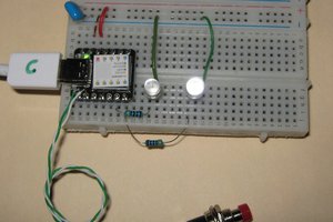
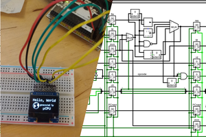
I had one green LED to play with, a 128x64 LCD to display some text/graphics,
and a accelerometer.
CURL worked as expected, that covered most of my Ethernet needs.
Next was creating FPGA peripherals for the HPS side.
I was able to control the 10 red LEDs and the 6 segmented LEDs, and do
some VGA stuff pretty easily.
The only draw back was that the synthesis time takes 10 minutes, so I'm more
motivated to use simulation with this board.
Generating a bare metal kernel.
The Intel FPGA Monitor Program doesn't provide files for the DE-10 SOC,
but I found what I needed under the Demonstration directory on the DE10 System CD.
.../Demonstration/SoC_FPGA/ControlPanel/Quartus/soc_system.sopcinfo
.../Demonstration/SoC_FPGA/ControlPanel/Quartus/output_files/DE10_Standard_FB.sof
In the Monitor Program wizard under system settings, pick the "Custom System" option.
and select the .sopcinfo and the .sof files.
The rest of the setup should be the same as the one Altera provided.
For my project I went the assembly route. This program blinks the green HPS LED.
.include "address_map_arm.s"

.text
.global _start
_start:
    BL    GPIO_SETUP

LOOP:
    LDR    R0,=0x08000000
LOOP_1:
    SUB    R0,R0,#0x01
    CMP    R0,#0x00
    BNE    LOOP_1
    BL    LED_G_ON

    LDR    R0,=0x08000000
LOOP_2:
    SUB    R0,R0,#0x01
    CMP    R0,#0x00
    BNE    LOOP_2
    BL    LED_G_OFF

    B    LOOP
.POOL

GPIO_SETUP:
    STMFD    SP!,{R0-R3,LR}

    LDR    R0,=0xFF709000
    LDR    R1,=0x00000000
    STR    R1,[R0]
    LDR    R0,=0xFF709004
    LDR    R1,=0x01000000
    STR    R1,[R0]

    LDMFD    SP!,{R0-R3,PC}
.POOL

LED_G_ON:
    STMFD    SP!,{R0-R3,LR}

    LDR    R0,=0xFF709000
    LDR    R2,=0x01000000
    LDR    R1,[R0]
    ORR    R1,R1,R2
    STR    R1,[R0]

    LDMFD    SP!,{R0-R3,PC}
.POOL

LED_G_OFF:
    STMFD    SP!,{R0-R3,LR}

    LDR    R0,=0xFF709000
    LDR    R2,=0x01000000
    LDR    R1,[R0]
    BIC    R1,R1,R2
    STR    R1,[R0]

    LDMFD    SP!,{R0-R3,PC}
.POOL
The LCD back light can be toggled with this code:
GPIO_SETUP:
    STMFD    SP!,{R0-R3,LR}
    LDR    R0,=0xFF709000
    LDR    R1,=0x00000000
    STR    R1,[R0]
    LDR    R0,=0xFF709004
    LDR    R1,=0x01000100
    STR    R1,[R0]
    LDMFD    SP!,{R0-R3,PC}

TURN_ON_LCD_LED:
    STMFD    SP!,{R0-R3,LR}
    LDR    R0,=0xFF709000
    LDR    R2,=0x01000000
    LDR    R1,[R0]
    ORR    R1,R1,R2
    STR    R1,[R0]
    LDMFD    SP!,{R0-R3,PC}
To wake up CPU core 1, use this code:
    LDR    R0,=0x00000002        // CPU1 Reset
    LDR    R1,=0xFFD05010
    STR    R0,[R1]

    LDR    R0,=0x00000000        // CPU1 Address
    LDR    R1,=0xFFD080C4
    STR    R0,[R1]

    DMB    ISHST            //Write MB

    LDR    R0,=0x00000000        // CPU1 Release
    LDR    R1,=0xFFD05010
    STR    R0,[R1]
Now that both CPU cores are active, we can use the
affinity register to have different CPU threads
    MRC    p15,0,r0,c0,c0,5
    MOV    R1,#0x03
    AND    R0,R0,R1

    CMP    R0,#0x00
    BEQ    CPU_0
    CMP    R0,#0x01
    BEQ    CPU_1
And for a good speed up, cache and branch prediction can be activated.
Both CPUs need to run this.
    MRC    p15,0,r0,c1,c0,0
    ORR    r0,#0x0004        // Data Cache
    ORR    r0,#0x0800        // Branch Prediction
    ORR    r0,#0x1000        // Instruction Cache
    MCR    p15,0,r0,c1,c0,0
 Reed Foster
 Altairish
 LambertTheMaker