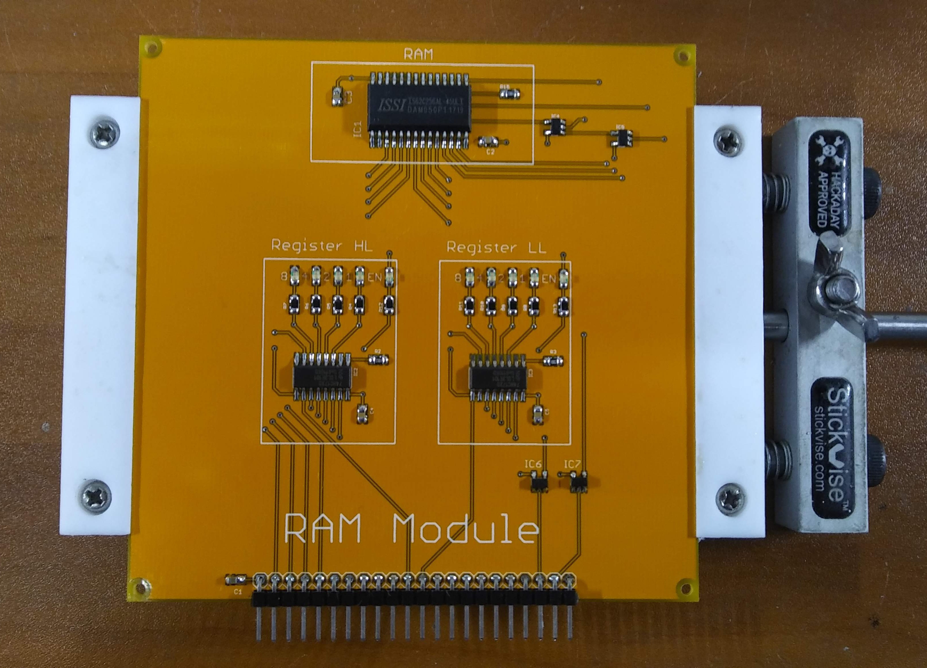
One of the fundamental items for a microprocessor/microcontroller system is the ability to have read/write memory storage. After carefully reading many of the datasheets for original 4-bit systems, it was apparently that many used either a latch or register to control the memory address access to the memory. In my design I've used two 74HC173D which are 4-bit wide. One is used for the upper 4-bits of the memory address, and another for the lower 4-bits. The memory itself is a 32K x 8 parallel SRAM chip (IS62C256AL). There are 4 LEDs on each 4-bit latch to indicate the stored value, and one LED to indicate when the latch is enabled. This module was initially designed and tested as part of an earlier project (4-Bit Architecture Experiments) to valid some of the DDL4 design. The only changes to the design were a bigger connector for future expansion, and the addition of Schmitt triggers (It Helps If You Know Your Schmitt!) on the system clock and reset signals.
 Dave's Dev Lab
Discussions
Become a Hackaday.io Member
Create an account to leave a comment. Already have an account? Log In.