-
Program Counter and ROM Testing
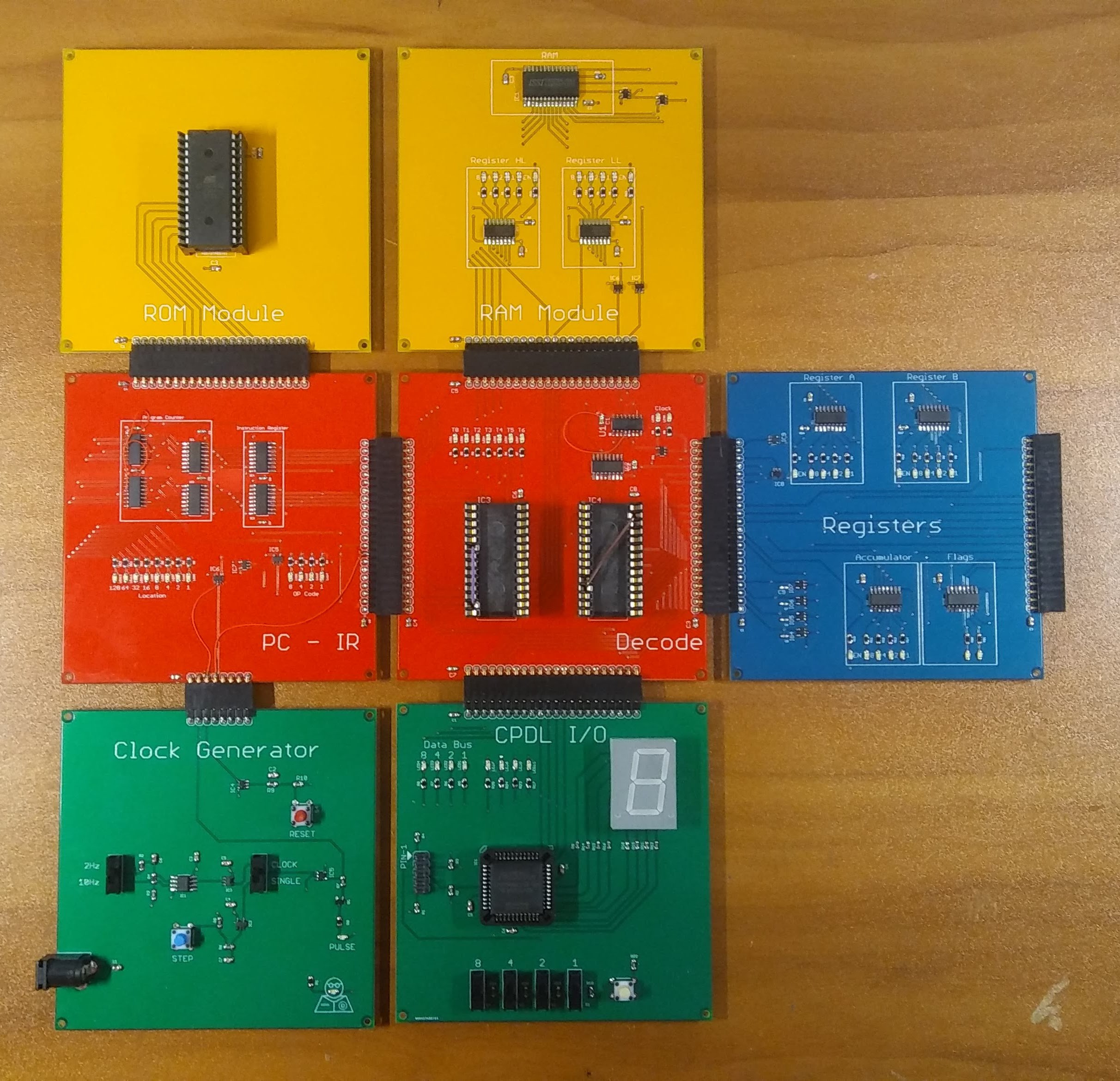
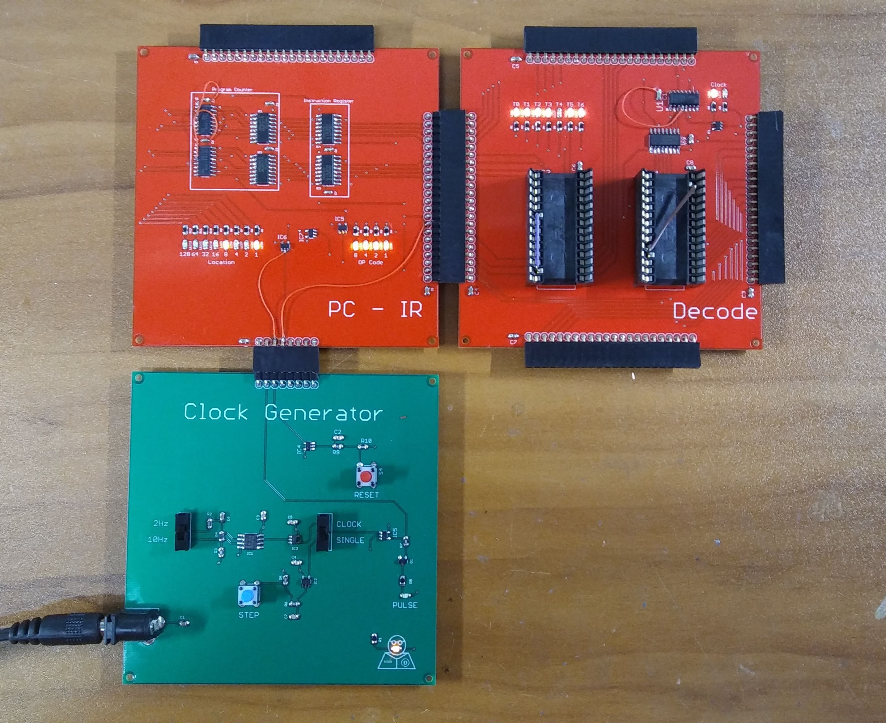
05/28/2018 at 21:23 • 0 commentsSo now that I have enough modules assembled to do some testing, I programmed the ROM with a series of test patterns to exercise the program counter, the OP Code Register, and the Immediate Data Register. The first 16 bytes of the ROM are programmed with 0 to F in the upper nibble which corresponds to the OP Code. The second set of 16 bytes of the ROM are programmed with 0 to F in the lower nibble which corresponds to the Immediate Data. The third set of 16 bytes, have both the OP Code nibble and the Immediate Data nibble programmed from 0 to F. This pattern helps identify any LSB/MSB signal swaps as well as make sure the ROM is reporting data from the correct address. In this video, I run the test first at 2Hz clock, reset the board, and then run at the 10Hz clock. At the end of the video, I demonstrate using the "step" button to pulse the system clock. So far things are looking good!
-
We Be Makin Progress!
05/26/2018 at 04:35 • 0 comments![]()
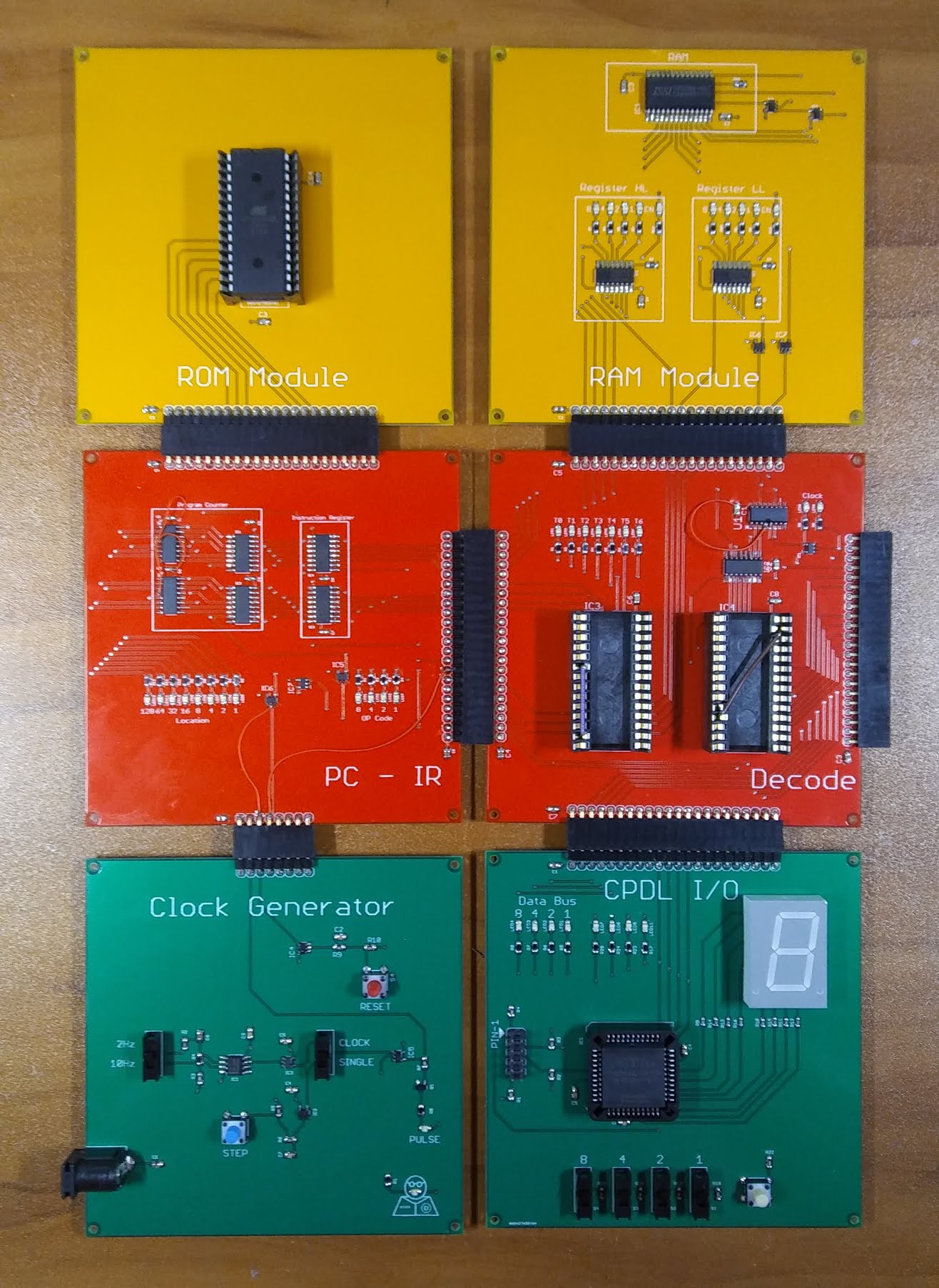
With the completion of the Registers Module, the only remaining board is the Mega-One-8-One ALU !!!! Then I can begin doing some incremental testing and programming of the EEPROMs for decode as well as programming the ROM for some test data....
-
Registers: Not the Cash Kind
05/26/2018 at 04:27 • 0 comments![]()
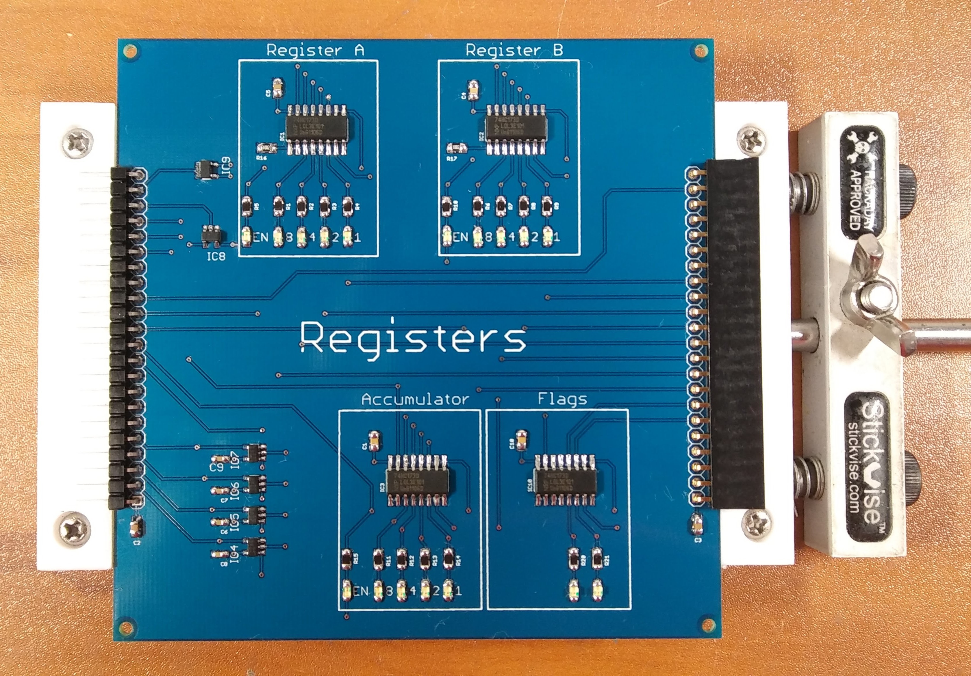
The assembly of the Registers Module is complete! The Registers Module started off as the ALU Module as part of the 4-Bit Architecture Experiments project. The ALU portion has been removed, leaving the A, B and Accumulator registers. Another 4-bit latch has been added to handle the ALU flags. Only two flags are currently being stored, but I was already using the 74LVC173D 4-bit latches for the A, B, and Accumulator registers, and it makes sense that in the future I might want to have additional flags. Each register has LEDs to indicate the contents and a LED to indicate when the register is enabled.
-
Six Down: Two to Go!
05/26/2018 at 01:06 • 2 comments![]()
Well.... I have six of the modules completed! The Registers Module is next on the assembly list. It is pretty straight forward assembly and is based mostly on the ALU module from the 4-Bit Architecture Experiments project. I removed the ALU portions from the board and replaced them with a 4-bit latch to hold the resulting arithmetic flags from the Mega-One-8-One ALU. The ALU portion of this project is the most tedious to assemble. The last prototype I assembled took three evenings to complete. There is nothing complicated about the board, there are just a LOT of components that need to be correct....
-
I/O: Off To Work We Go!
05/26/2018 at 00:58 • 0 comments![]()
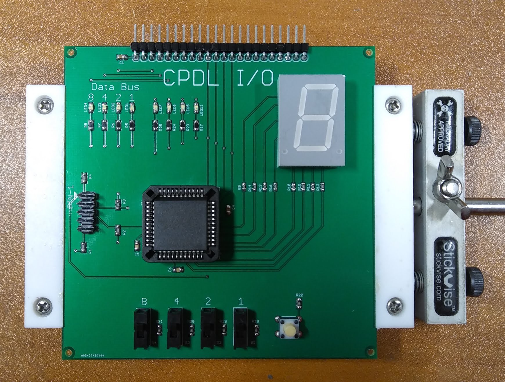
I have to admit using a CPLD for the I/O Module feels like a bit of a cheat, but I already had this design completed as part of the Digital Design Doohickey project. I hope to replace this with something more appropriate later on down the road. The design includes some LEDs for display the data that is currently being presented on the 4-bit Data Bus. The CPLD is directly connected via the I/O pins to a 7-segment display, 4 LEDs, 4 switches, and a push button. The CPLD is programmed via a 2x5 JTAG header on the board. The Altera EPM7064SLC44-10N is a costly part (around $9.00USD at digikey), and is a End-of-Life project. I already had some on hand, and the board was already designed, so I decided to use it for now. The design is loosely based around a post made on a Hackaday a while back called "A Better Way to Plug a CPLD Into a Breadboard".
-
Debug Time...
05/25/2018 at 23:21 • 0 comments![]()
With the Clock Generator Module completed, I was able to begin debugging some of the modules. The PC-IR Module and the Decode Module are the only two modules in the design that were not previously tested as part of another project, so they were my first concern. Both the PC-IR and Decode Modules use a 74LVC193D, which I had not previously used in a project. Unfortunately, I didn't read the datasheet closely enough. I am not using the "down" could features of the 74LVC193D, so I tied it to ground. WRONG! Apparently when the down count is not used it needs to be pulled to VCC. I added wire fixes to both the PC-IR and Decode Modules. After adding some jumper wires to the EEPROM sockets on the Decode Modules to allow for testing, I powered up the boards.... and nothing. The Clock Generator wasn't running. I had already tested the Clock Generator, and knew it was working, but what could be the problem? Turns out the RESET and HALTn signals had gotten swapped on the PC-IR modules, so a second set of wire fixes were needed. After doing a bit of soldering, I was ready to re-test. BINGO! I have the phase counter working, as well as the program counter! Time to move on to assembling the remaining modules!
-
Clock: A Good Time
05/25/2018 at 23:13 • 0 comments![]()
So the Clock Generator Module is assembled! Well... this is actually the second one I assembled. Last night I finished the first one and cleaned it in my heated ultrasonic cleaner, and then placed it in my reflow oven to dry it off. I have a pre-programmed "dry cycle" that heats the board to 105C for 2 minutes to dry up any moisture left on the board. Unfortunately, I wasn't paying attention and set it for a full "lead-free reflow cycle". I can back to check on the board just in time to smell plastic. After a cool down, I inspected the board.... every piece of plastic was melted... the buttons, the barrel jack, and the switches. In addition, it had reflowed the parts and there were a bunch of shorted pins! So I eneded up building another today. The Clock Generator Module was originally tested as part of the Digital Design Doohickey, and has basically remained unchanged, with the exception of added a reset button with a Schmitt trigger. The core is based on a 555 timer, and a Single-Pole-Double-Throw(SPDT) switch that lets me select a predefined clock rate of 2Hz or 10Hz. There is also a SPDT that allows me to use a step button connected via a Schmitt trigger to manually pulse the clock. A standard 2.1mm barrel jack provides a +5V input. I have a LED to indicate system power, and for the system clock pulse.
-
Four Down... Four To Go!
05/25/2018 at 01:58 • 0 comments![]()
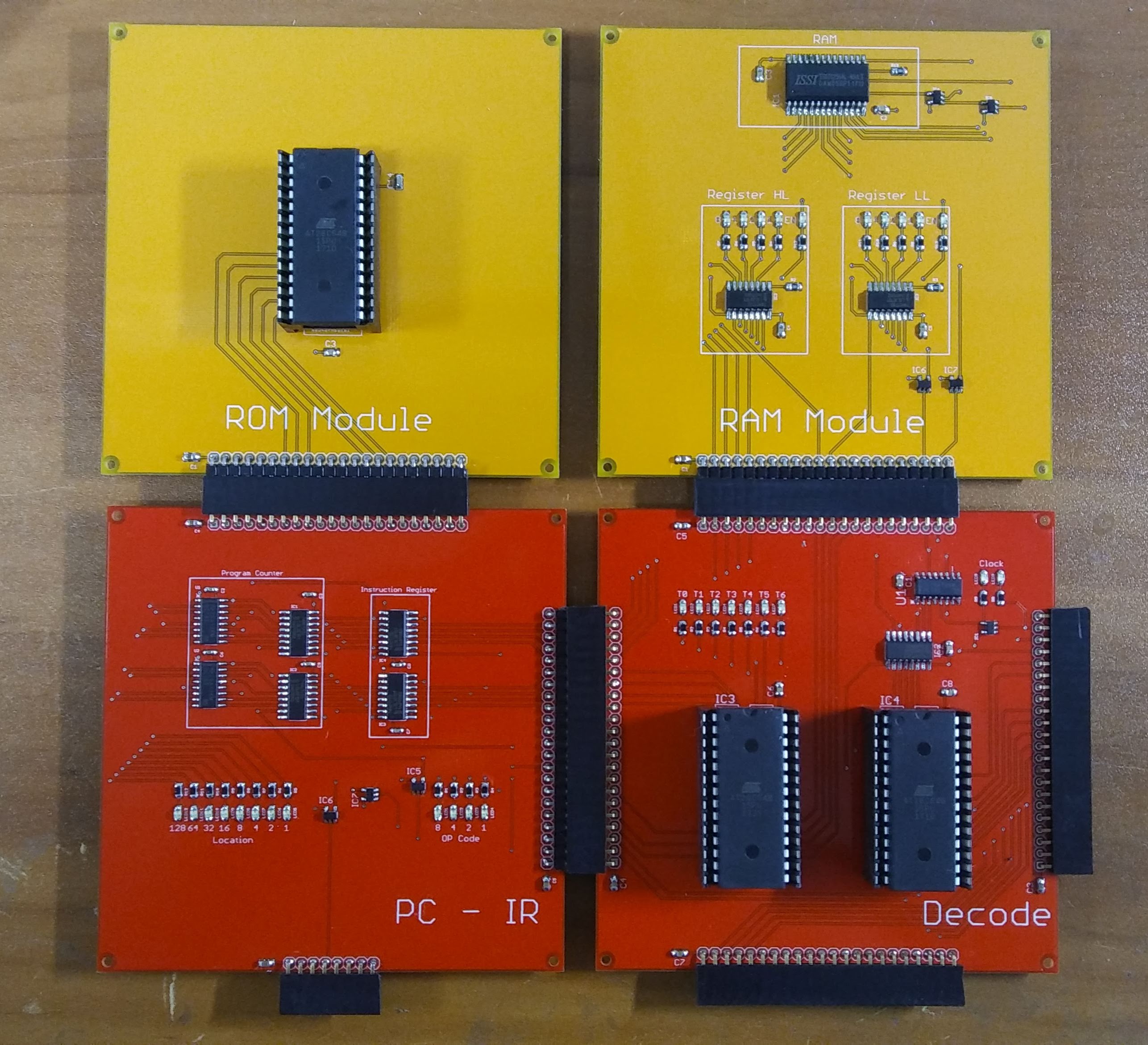
With the addition of some rubber feet to each of the modules, the first four are assembled!
-
RAM: Don't Forget Me!
05/25/2018 at 01:56 • 0 comments![]()
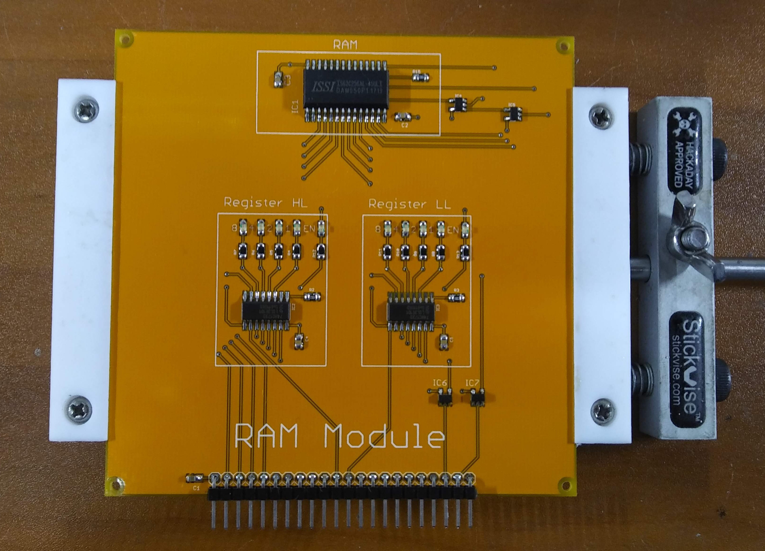
One of the fundamental items for a microprocessor/microcontroller system is the ability to have read/write memory storage. After carefully reading many of the datasheets for original 4-bit systems, it was apparently that many used either a latch or register to control the memory address access to the memory. In my design I've used two 74HC173D which are 4-bit wide. One is used for the upper 4-bits of the memory address, and another for the lower 4-bits. The memory itself is a 32K x 8 parallel SRAM chip (IS62C256AL). There are 4 LEDs on each 4-bit latch to indicate the stored value, and one LED to indicate when the latch is enabled. This module was initially designed and tested as part of an earlier project (4-Bit Architecture Experiments) to valid some of the DDL4 design. The only changes to the design were a bigger connector for future expansion, and the addition of Schmitt triggers (It Helps If You Know Your Schmitt!) on the system clock and reset signals.
-
PC-IR: I'm Counting on You!
05/25/2018 at 00:28 • 0 comments![]()
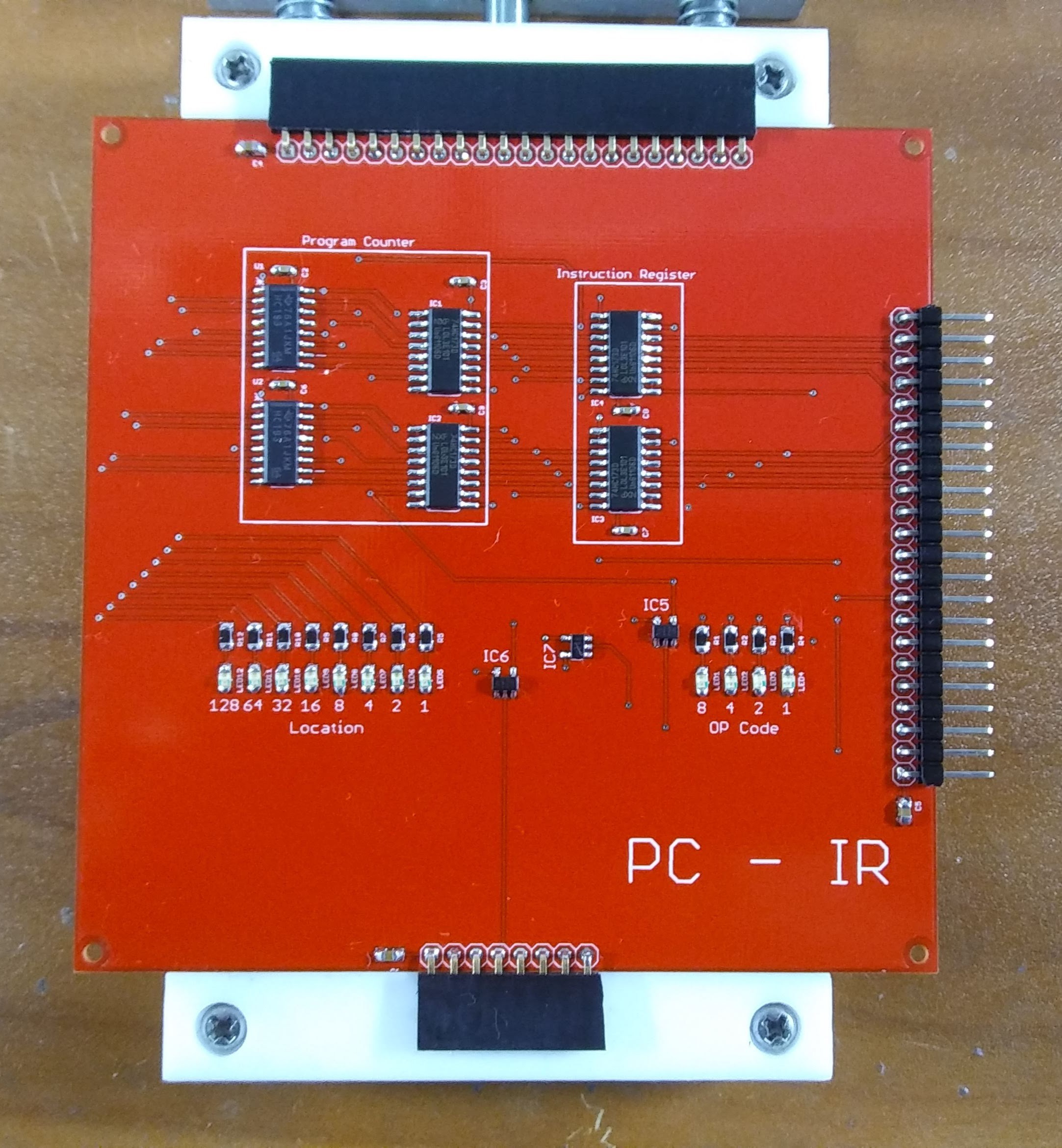
The PC-IR Module contains the 8-bit program counter and the 8-bit Instruction register. To make this design reasonably useful, I really needed an 8-bit program counter. This is implemented with two 74LVC193D 4-bit counters tied together. Because the design is intended to use some two cycle instructions, the program counter fed into two 74LVC173D 4-bit latches. This will be discussed in more detail later. I've included LEDs to indicate the current value of the program counter. The instruction register is also created using two 74LVC173D 4-bit latches. This allows the instruction set to use 8-bit wide instructions, which are 4-bit opcodes with 4-bit immediate values. I have also included LEDs to indicate the current 4-bit opcode. Because the system clock and reset are passed through this board to other boards, Schmitt Triggers have been added on those signals to deal with possible noise and current limitations.
 Dave's Dev Lab