Memory and Instruction Fetch
Here are some Logisim subcircuits representing parts of the machine
concerned with memory, instruction fetching and instuction decoding.
Main Memory
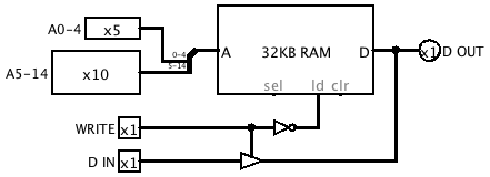
Although the memory in the final machine will be dynamic, I'm modelling
it with a Logisim static memory component for now. The memories I
intend to use have asynchronous write with separate data inputs and
outputs. but Logisim doesn't provide that combination directly, so I
emulated it using a tri-state buffer.
I split out the address bus inside the subcircuit into bit number
(A0-A4) and short word number (A5-A14) parts, to make the main circuit
clearer.
Program Counter
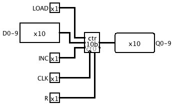
The Program Counter is a 10-bit counter with Increment and Load capabilities, both synchronous.
S Register
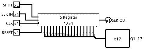
The S Register is an 18-bit shift register. The most significant 17
bits are available as parallel outputs for loading into the Instruction
Register.
Why the most significant rather than the least significant? That's a
good question! It's because the Instruction Register will be loaded
during the last clock period of a memory read cycle, when the most
significant bit hasn't yet been shifted in. Therefore, at that time,
bits 0-16 of the instruction word will be in bits 1-17 of the S
Register.
Instruction Register
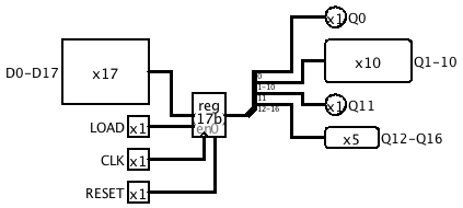
The Instruction Register is fairly simple -- it's just a 17-bit
register with synchronous parallel load. The subcircuit splits the
output into instruction fields: Length (0), Address (1-10) and
Opcode (12-16). (Bit 11 is currently unused.)
Microcode ROM
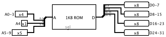 There's not a lot to see here either. I'm not sure exactly how wide the microcode will need to be, I've made it 32 bits for now.
Bits 4-9 of the microcode address will come from the instruction, and
bits 0-4 from the State Counter. Thus, each combination of Opcode and
Length will select a line of microcode with room for up to 16
microinstructions.
Putting it together
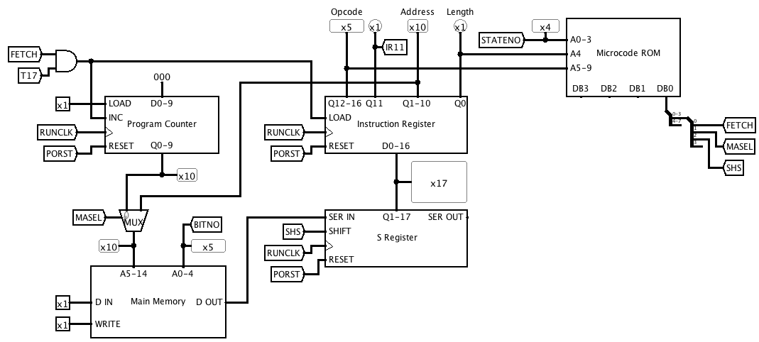
Here's how it goes together so far. Fetching an instruction is
accomplished by setting FETCH = 1, MASEL = 0 and SHS = 1. This causes
the main memory address to be taken from the Program Counter, and data
read from the memory to be shifted into the S Register. FETCH together
with T17 causes the Instruction Register to be loaded from the S
Register, and also increments the Program Counter ready for fetching
the next instruction.
Discussions
Become a Hackaday.io Member
Create an account to leave a comment. Already have an account? Log In.