 Mile
MilePCBs for this project were designed with ease of reproducing in mind. Main goal was to achieve smallest size as possible to reduce the cost of fabrication while still being relatively easy to assemble. Components used are in SOT, SOD, 5050 and 0603 packages. Hardest components to solder are SOT packages because. Switching converter in bigger packages just aren't available. Tight layout of components is necessary to ensure optimal operation of switching converters. 3D preview of the module.

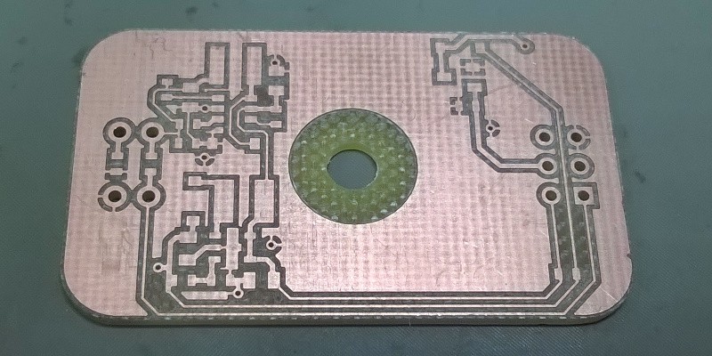
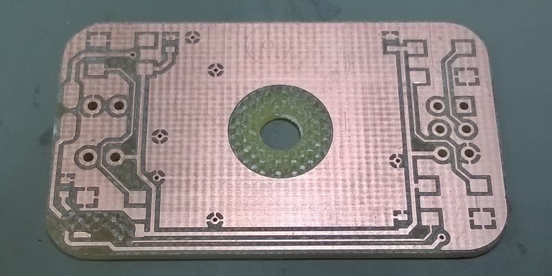
To make assembly process easier assembly drawing is included. Bottom pictures show milled PCB (bottom and top side). Some traces are damaged so I will have to repair them with jumper wire.
Discussions
Become a Hackaday.io Member
Create an account to leave a comment. Already have an account? Log In.