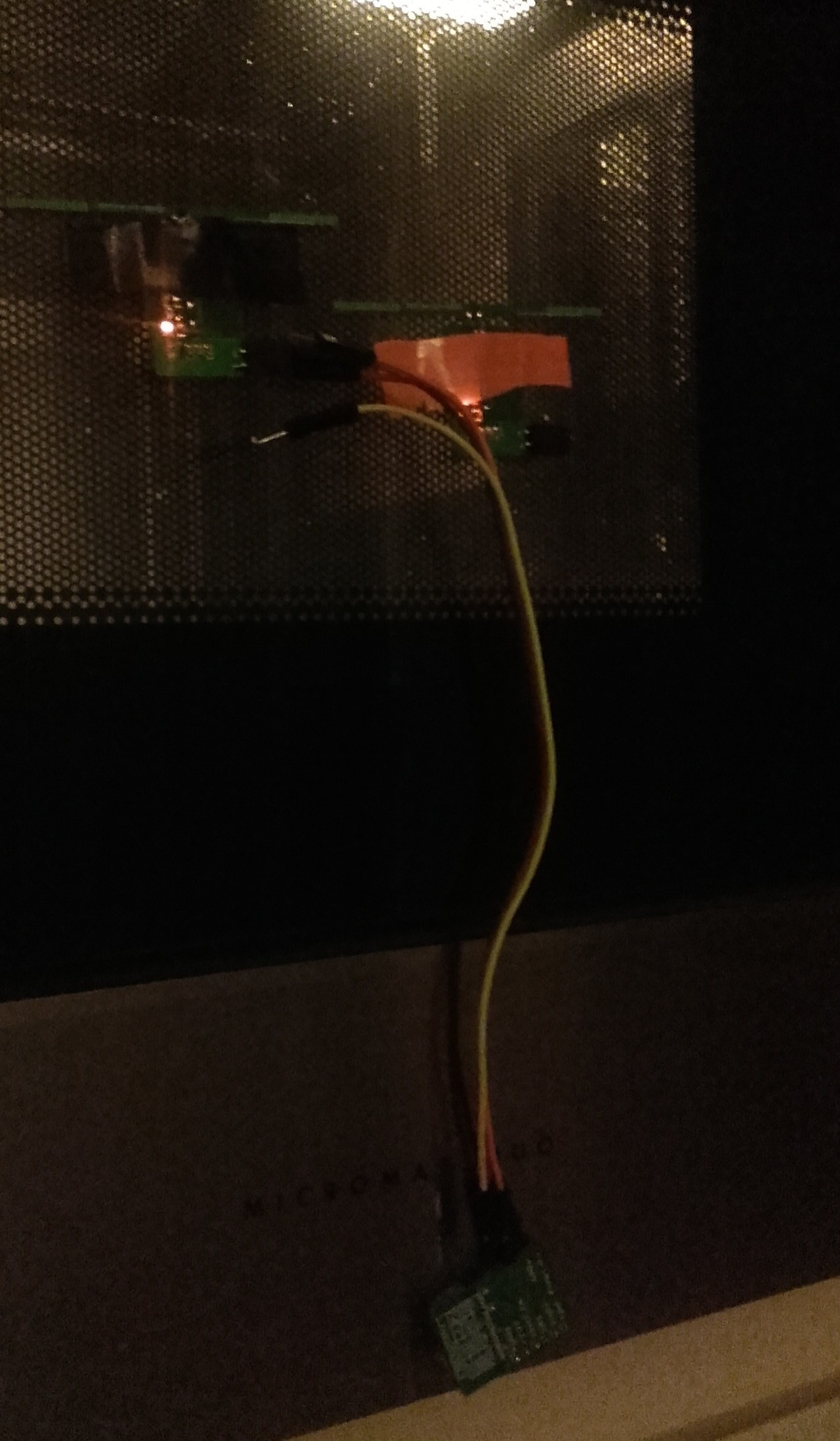
As you've seen in previous logs, I managed to get done 2 things:
1) get RF-detecting PCB (further in this text - PCBA-1) working, so that even LED is flashing, when sticked to mW-oven.
2) get energy-harvesting (further in this text - PCBA-2) IC working, so when there is ultra-low voltage power source, the buffer capacitors are charging.
I thought, obviously, now I just connect these two PCBAs together, and everything works!
Well.... I was wrong! :D - nothing worked as expected! - the capacitors at PCBA-2 are not charging at all.
I've made various assumptions, why this could happen (and what can be done to check if it's true):
1) When PCBA-2 with it's headers is inserted into socket of PCBA-1, the leakage radiation, which powers PCBA-1, also influences power inductor, placed at PCBA-2, or other it's components, therefore it malfunctions. (Then I've tried to connect PCBA-1 to PCBA-2 using two long wires, so I can place PCBA-2 outside mW-oven's window... Nothing changed - same problem....)
2) adding extra wires and/or PCBA-2 to PCBA-1 detunes it. (Then I've tried to connect only wires to PCBA-1- LED is still glowing... then wires have no influence... I've connected PCBA-2, only GND-wire, to check if it's GND plane detunes PCBA-1.... the answer was "no" - LED was still glowing)

3) Considering two previous points, I conclude, that energy-harvesting circuit has such a low efficiency, that tiny amount of energy, detected by PCBA-1, is wasted almost totally.
As result, I have following action-plan for next 2 weeks:
1) It's obvious, that if there is enough voltage and energy, generated by PCBA-1, to light up a LED, then there will be enough voltage and energy to power MCU+BLE.
2) Then, the only challenge is to store ALL possible energy, without losing it, before using it. When stored energy is enough to send message, start using this energy (maybe even using ultra-efficient buck-converter). This could be achieved, by increasing output capacitance at PCBA-1 and adding special circuit, that activates main, more "energy-hugnry" circuits after some threshold. Similar approach is perfectly described here - https://hackaday.io/project/159691-electron-bucket-extreme-power-management-module . mWessenger-s circuit has same energy budget, but much higher power budget, therefore "triggering"-circuit may be done simpler (more leakage allowed). =)
3) The drawback of bigger capacitance add-on would be lower average voltage of system (if it's supercap with tenths of Farads, voltage probably would never reach more than 1V). Anyway, I see, that boost-converter would be still required, after voltage at supercapacitor drops below MCU's minimal VDD. In this case I would redesign PCB, responsible or energy harvesting, by replacing LTC3108 with some more power-efficient IC. Some examples: BQ25570 / BQ25505 / BQ25504 from TI. I'll study later also other companies' products and select the most efficient and feature-rich.
So... plan is ready, - action!.
P.S.> Oh!... one more idea: use one main capacitor for energy storage, and some extra "switchable" capacitors - when the first cap overflows, some logic connects next capacitor, using MOSFET, therefore reducing system's voltage by some amount and allowing system to store more energy....
 Jurist
Discussions
Become a Hackaday.io Member
Create an account to leave a comment. Already have an account? Log In.