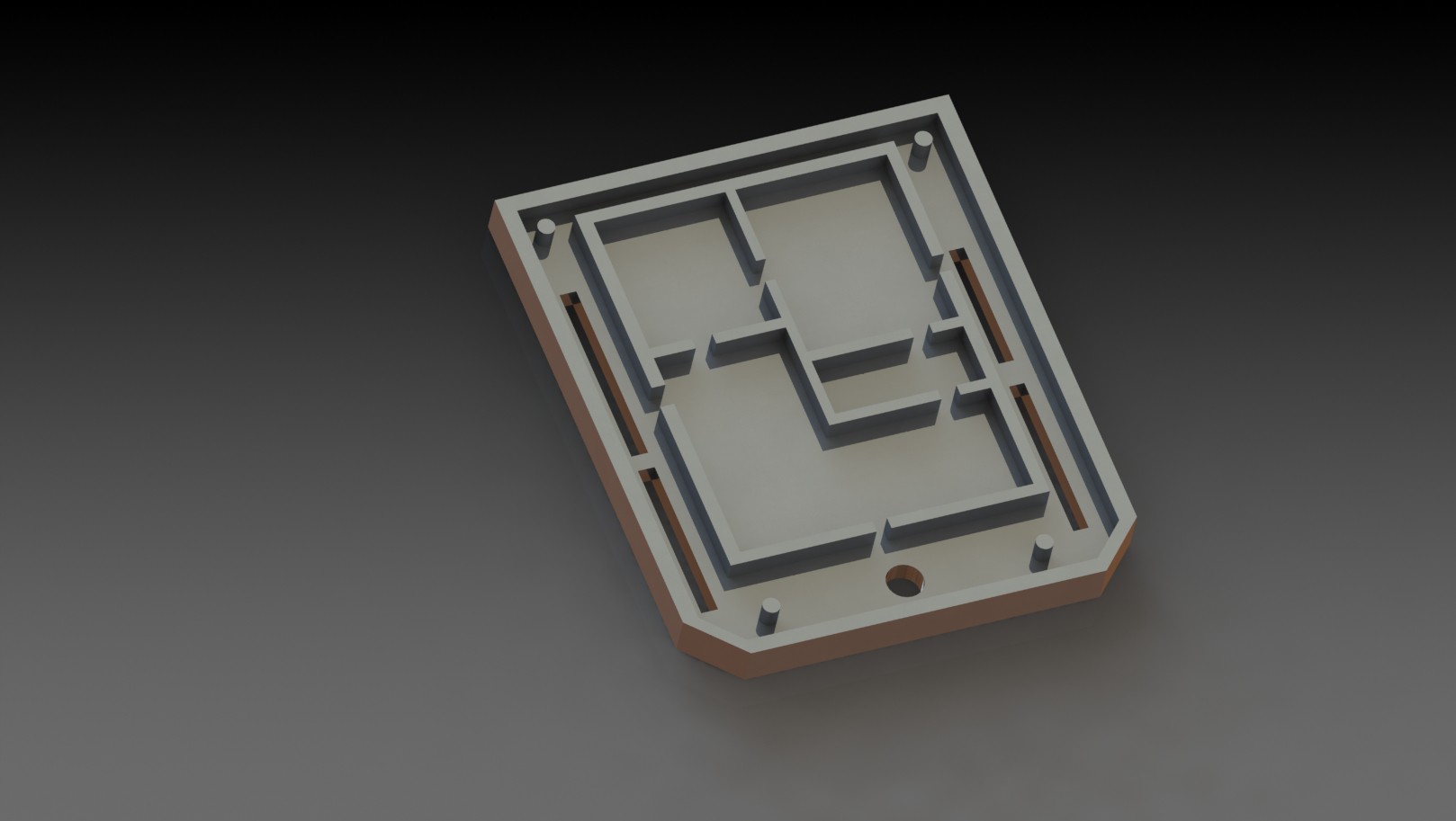
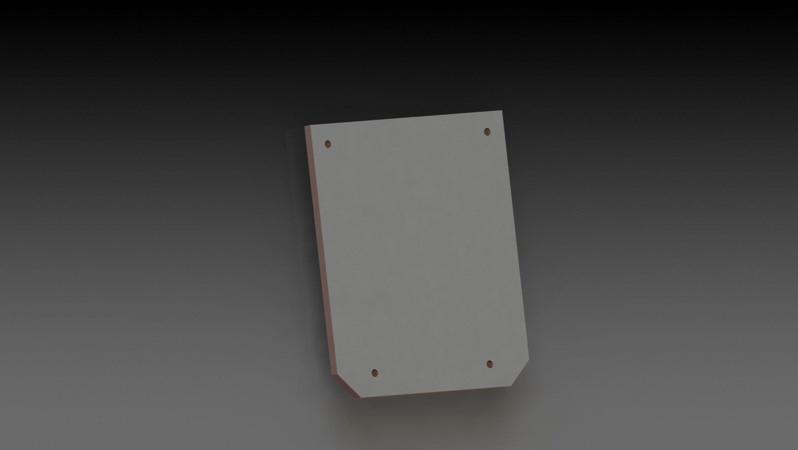
I threw together some quick drawings of what the final product may look like. This is my "artists representation". I tried to make design choices that made sense and that kept the design manufacturable. So here's what I came up with:
A couple things to note: not all the parts in these drawings are exactly to scale yet, and the exact dimensions will change based on the layout in the next iteration. The basic design is two parts that fit over the PCB, held together by 4 screws. There are several purposes this enclosure serves:
1) Protection against the elements and ESD damage from casual handling of the board.
2) Thermal relief for the circuit, since the entire enclosure is manufactured from aluminum and acts like a heat sink. This design should be able to be die cast, which will make it more manufacturable. Ideally this would be 7000 Aluminum, but I'm not sure if that's capable of being die cast.
3) Shielding for spurious radiation and interference from outside
4) Shielding for spurious radiation and interference from inside (caused by the circuit itself). Both 3) and 4) are very important in passing FCC emissions testing, so I'm hoping this (along with certain layout techniques) will keep this design FCC Part 15 compliant.
5) Shielding for self-interference. The raised channels on the inside of the first drawing will make direct contact with trace fences on the PCB. This effectively creates a tiny shield around each section of the circuit. This is important because this design uses heterodyning to generate frequencies, so there will be multiple copies of signals at different bands and amplitudes, plus harmonics, all very close to each other. Fencing in the CC430, ADF4351, mixer, and front end will prevent crosstalk and reduce noise and harmonics on adjacent traces.
I didn't want to design an enclosure that kept the user out though, so all you have to do is remove 4 screws and you can probe or modify the PCB however you want. I didn't include it in the rendering, but to help make this design more understandable, there will be silkscreened labels on the top of the enclosure beside the pins to identify each pin number and function.
Once I get the next revision done, I'll get a prototype of this 3D printed in at least plastic, maybe metal. I may also play with the aesthetics a little and try to use depth more. I don't want to design anything that can't be achieved with die casting, but I think there are still some things I can get away with.
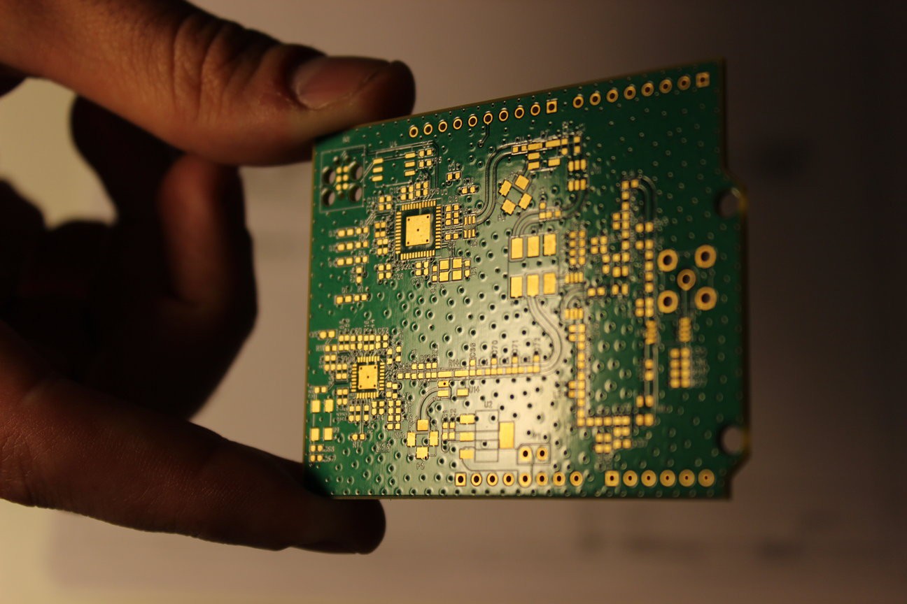
While I'm on the subject of productization, one of the often overlooked problems with getting an electronic product to market is FCC certification. Part 15 says that a device can't cause interference and must accept any interference it encounters. There are lots of good design practices used to help meet this certification. For example, having lots of easy paths to ground prevents stray inductance from occurring. That's why there are so many vias on the board:

I don't know if this will pass EMC testing, but I'm keeping it in mind and I'm hoping the combination of good layout techniques and the enclosure will make passing it easier.
 Hunter Scott

Discussions
Become a Hackaday.io Member
Create an account to leave a comment. Already have an account? Log In.