After some diversions on other work I'm finally getting around to working on the TS350's redesign again. I did a poor job on the original thermal model and didn't account for the increase in Rds(on) of the MOSFETs (with temperature) and, more importantly, the coupling of adjacent components. The result was that the inverter section would overheat (shutdown) at continuous operation much above a 300W output.
One of my enlightenments after some additional book work is the need for thermal imaging to get a true picture of what's going on; my spot IR thermometer & thermocouples don't cut it. I picked up a FLIR One Pro. Because it uses a smartphone for display & processing it's half the cost of an entry level professional, self-contained, IR camera.
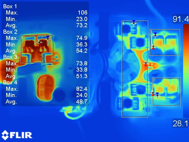
It's easy to use and with the companion FLIR Tools application enables you to quickly analyze image data. Here's an image of the TS350 powering a 300W load continuous. The temperature boxes were added after the image was taken with the Tools appl.
The camera paid for itself on the first use. Revelations:
- Box 1: the high-side sine switches run much hotter than the low-side, even though they are on only half-time (vs. the low side on ~ 85% of full sine cycle). Why? Because the high side experience high voltage & current switching stress (at turn on there is a +170V gradient D-S) whereas the low side switches under near 0V conditions. A secondary contributor is the higher thermal coupling coefficient of the high-side transistors since adjacent to one another. Duh.
- Boxes 2 & 3: my model over-estimated the temperature rise of the relay MOSFETs. I didn't install heat sinks and they are running close to my model's predicted temperatures with heat sinks. Also note that the temperatures between the +/- poles are symmetrical (good).
- Box 4: thermally speaking the inverter MOSFETs are my problem child but at first glance the image doesn't reflect that. The hot spot in the box are the current sense resistors and, while not a surprise, is a reminder to be careful with their location and coupling effects to & from them. Heat sinks are installed on the switches and they are quite cool. But most of the board area around them is copper and the image shows those temps >70C. My conclusion is that the heat sinks do a poor job of conducting heat from the board and that leads to high case / junction temperatures. As with the sine MOSFETs, the coupling effect doesn't help.
My take-away is that SMD heat-sinks are okay when dealing with only a few watts for a single device but for higher powers & multiple devices they are inadequate. I suspect they can also present a significant near-field capacitive coupling problem with few remediation options other than a shielded enclosure.
So, for the redesign I am creating a linear superposition model that will account for coupling effects. To do this requires that I know the coupling coefficients and these must be measured from a thermally representative model of the design. All of this implies that I need to make decisions on the board layout, transistor mounting, heat sinks, etc.
I'm definitely gong with TO220 MOSFETs for the inverter with the goal of a more compact footprint and improved thermal efficiency. The relay will remain SMD but will probably offload to a separate power board that contains the power connections, user interface, etc., and because of this probably won't need heat sinking. I haven't decided on the sine section yet. From an EMI perspective it needs lots of improvement and much of it will revolve around reducing the size of current loops.
Lots to do!
Discussions
Become a Hackaday.io Member
Create an account to leave a comment. Already have an account? Log In.