 Nicolò
The
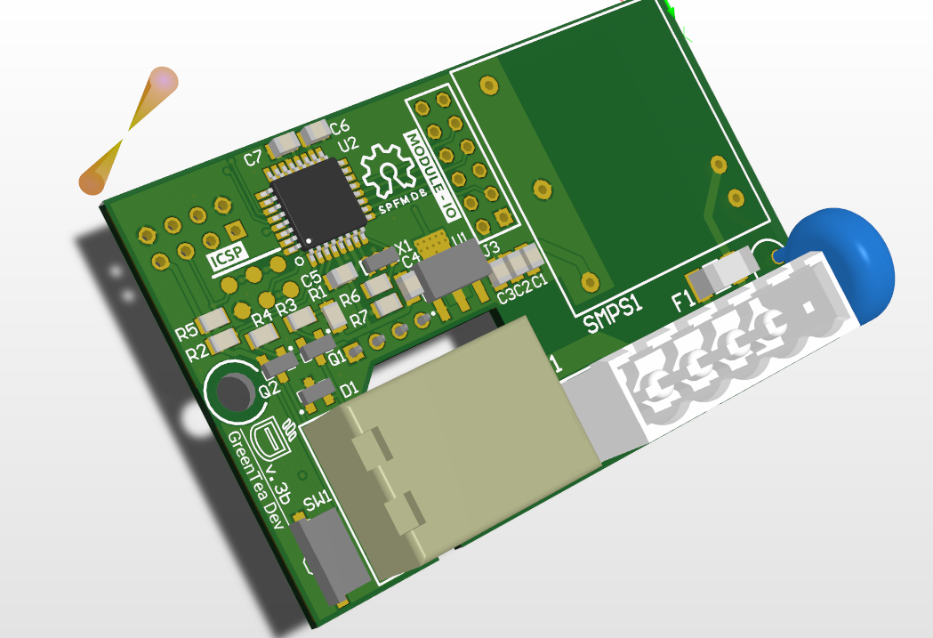
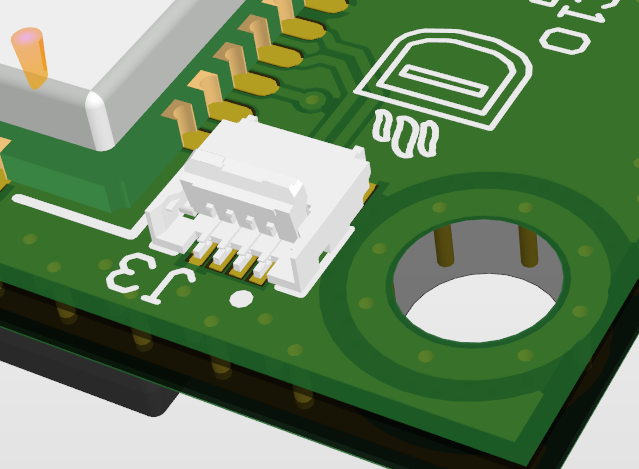
The baseboard now have the the Atmega on the top side, one of the mout hole has been removed. In this way I have more space to route stuff on both the baseboard and on modules.
The baseboard had a mirrored footprint for the SMPS, I have fixed that and in the meanwhile I rerouted the whole board! The main bg differenc of this layout that the connector of the module io now is connected to the main I2C bus in that way the front board can directly manage the shield without sending commands through the slave Atmega. The Atmega only works as a dummy IO Expander and Serial Bridge in case something need to be accesed by serial
 Also the programmer has been modified, now it have a built in USB to serial converter in this way I can program the Atmega with both the bootlaoder and the firmware itself.
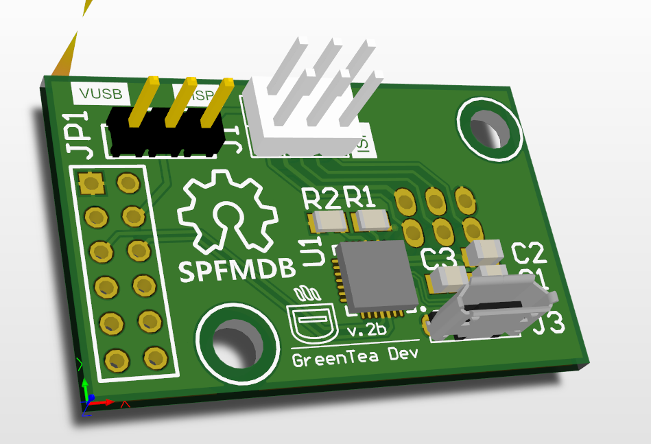 The board have a jumper to select the voltage source in this way I can use the 3V3 regulator inside the CP2102 or the one that is inside the ISP programmer.
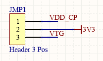 I have also reworked the SIM module, now it should work without problems. I have added more vias to shield it and with the tips from Raúl I created this layout:
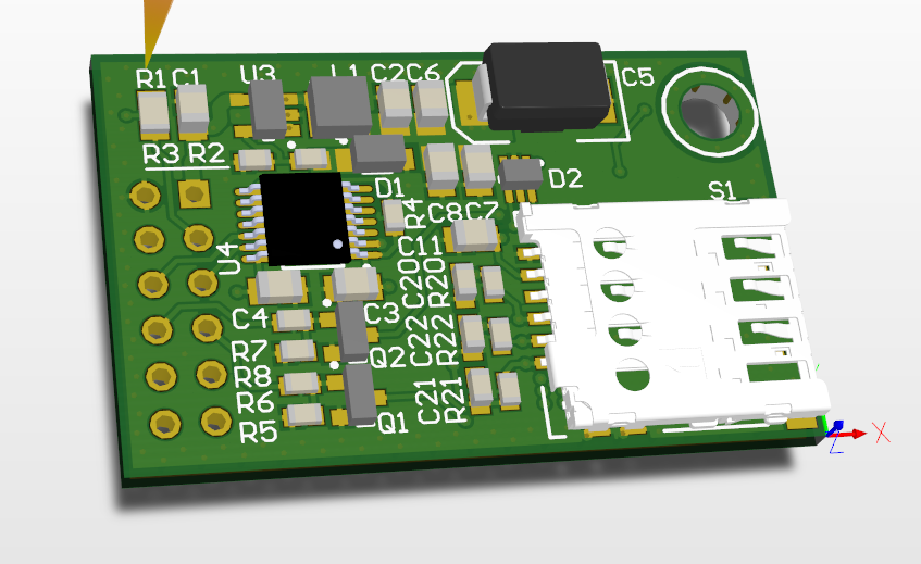 This one have all the necessary components for the SIM holder, and the PI network on the antenna. The big step was to replace the 0805 components with 0603. (With the exceptions of some caps in this way I can use the one I have at home). The GSM board now is a 4 Layer one, so the tracks for USB and the antenna have the right impedance!
Now the GSM moduel have also the USB routed out to a FPC connector! In this way I couldmake the front board capabel to connect to the internet instead of just sending SMS! (I still have no idea how to enable the USB on the SIM module)
Discussions
Become a Hackaday.io Member
Create an account to leave a comment. Already have an account? Log In.