Nicolò
-
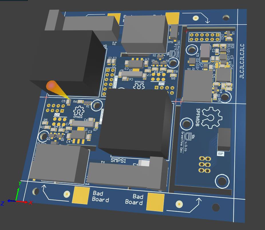
Small update, more testing. Wrong PCBs
08/29/2018 at 22:01 • 0 commentsHi guys,
sorry for my poor english.
This is just a quick update on the project:If you have any idea on what to do with the wrong PCBs write a comment!
-
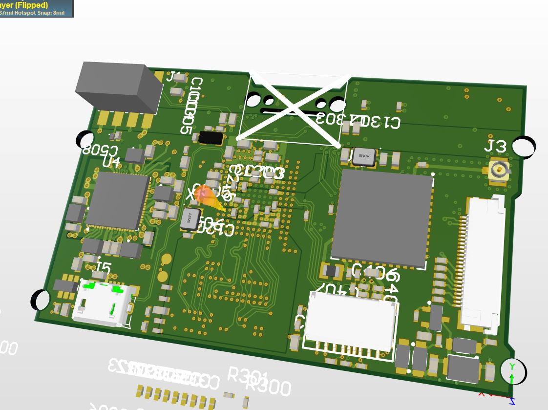
Testing out a new CAD
08/24/2018 at 15:03 • 0 commentsHi, right now My main PC is DOWN due to a failure on my graphics card. I think that some memory chip is fried!
Talking about memory I finally madeout how to route the memory lines for the DDR3 IC I'm using.
All the work done so far has been made on Circuit Maker. But I wanted to test out Altium Designer. So I just downloaded the trial and imported my project.
I tried out X-Signals and some other functions like the active routing but I'm not able to wake them work. Or at least not like on the advertisements videos...
![]()
You can take a look of the work I'm doing now. I'm still learning how the impedance control works: because on my calculations I get a track too wide to be routed under the BGA balls!
![]()
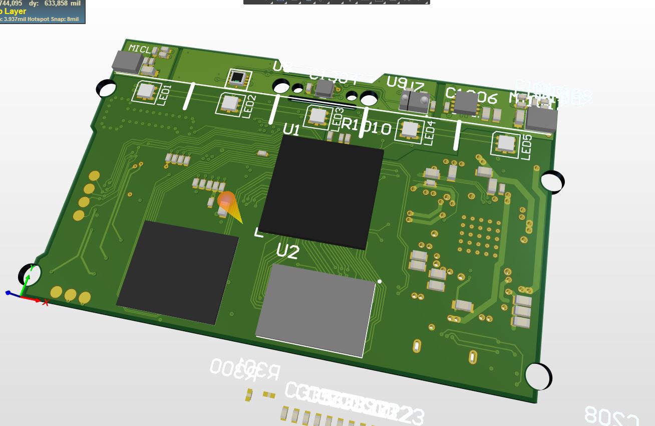
Now I'm trying to compress the power section, the power driver of the EPDand the USB protection circuit. So I can finally try to lenght match the tracks of memory. Now I have no space! (The pcb has 8 layers but it's not big enough)
-
I guess when it rains, it pours.
08/23/2018 at 08:18 • 0 commentsNot a lot of progress due to my PC failure when went back from holiday.
I'm waiting for some replacement parts.
I was not joking about the fact that I brought the soldering station on holiday!
Clothes, cable ties, Arduino box with some random porototypes, the mouser package with the components I was waiting. The soldering station. -
"Stuff happens": I made a huge mistake
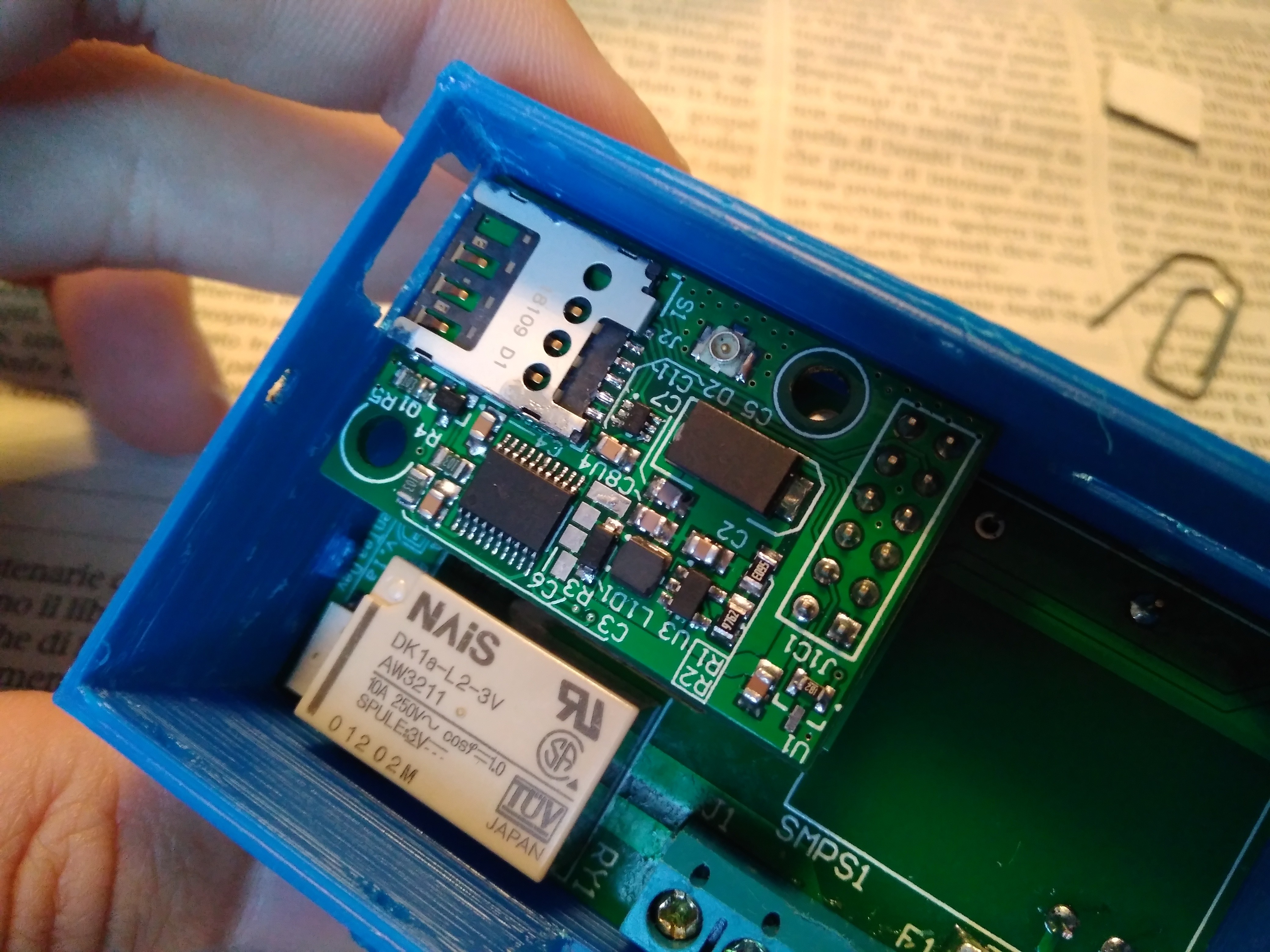
08/17/2018 at 21:27 • 0 commentsToday the package I was waiting has been delivered. I'm in a remote location so it's ok for me to wait a lot of time.
Unfortunately I don't had lot of time to develop the software. But I have played a bit with my Hakko soldering station that is with me in those holidays.
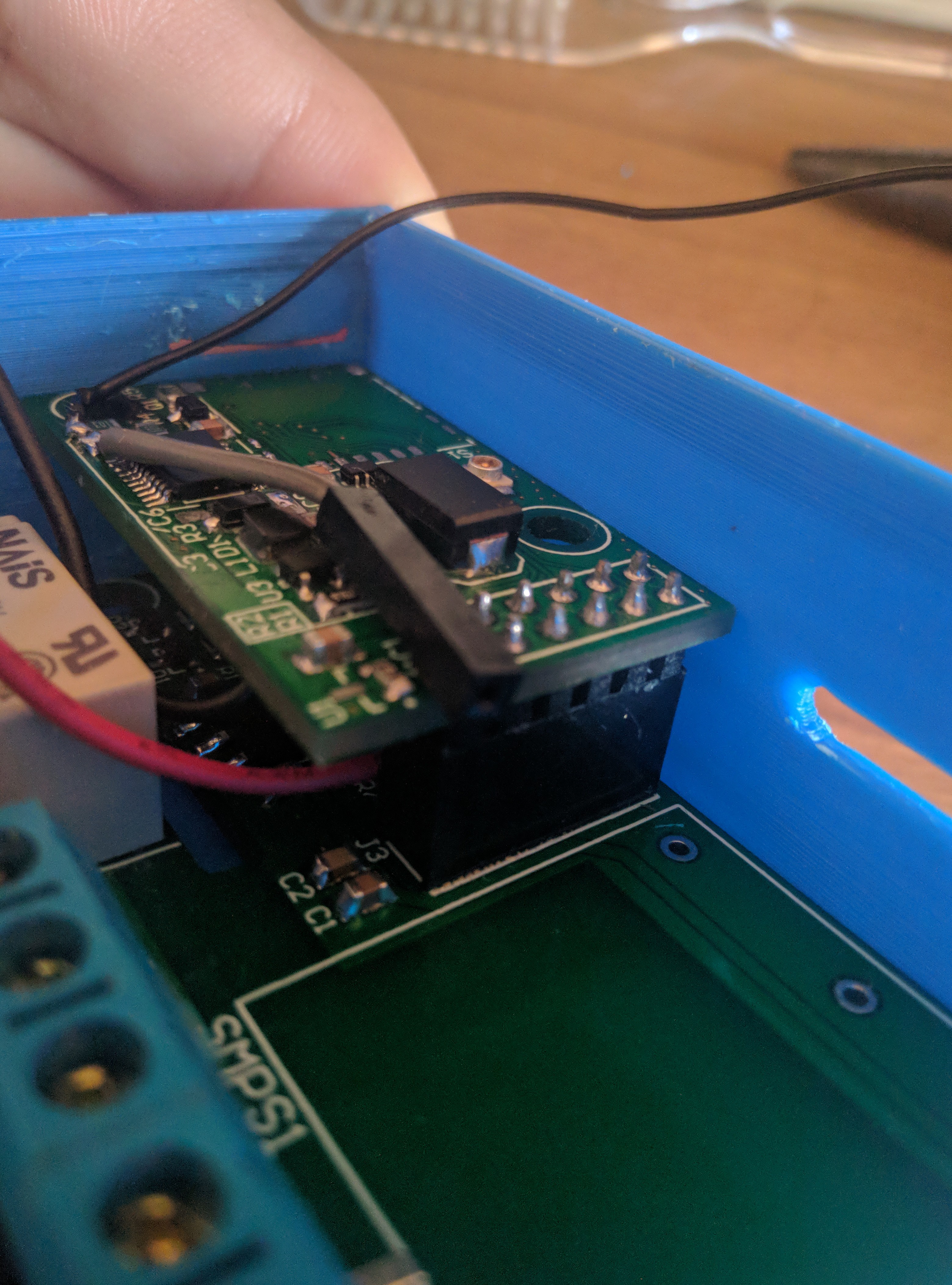
As you can see I have done the footprint for the SMPS upside down.
![]()
At least the Sim tray is working fine, it is not a spring loaded one due to the small space that I have available.
![]()
For today is all folks! I will be back at home in the next few days so I will develop and test some more stuff the next week!
-
Time to relax: Writing some software
08/04/2018 at 07:56 • 0 commentsHi guys, today I go on holiday, so I can't do much. So I can't do much in the next fiew days.
I'll be working on some drivers for this project and I'll write some code for the baseboard: it has to work as i2C slave. So I have to plan the registers and the general functions!
In the meantime I can relax and take a fiew stap back from this mess:![]()
You guessed, it is the front board! -
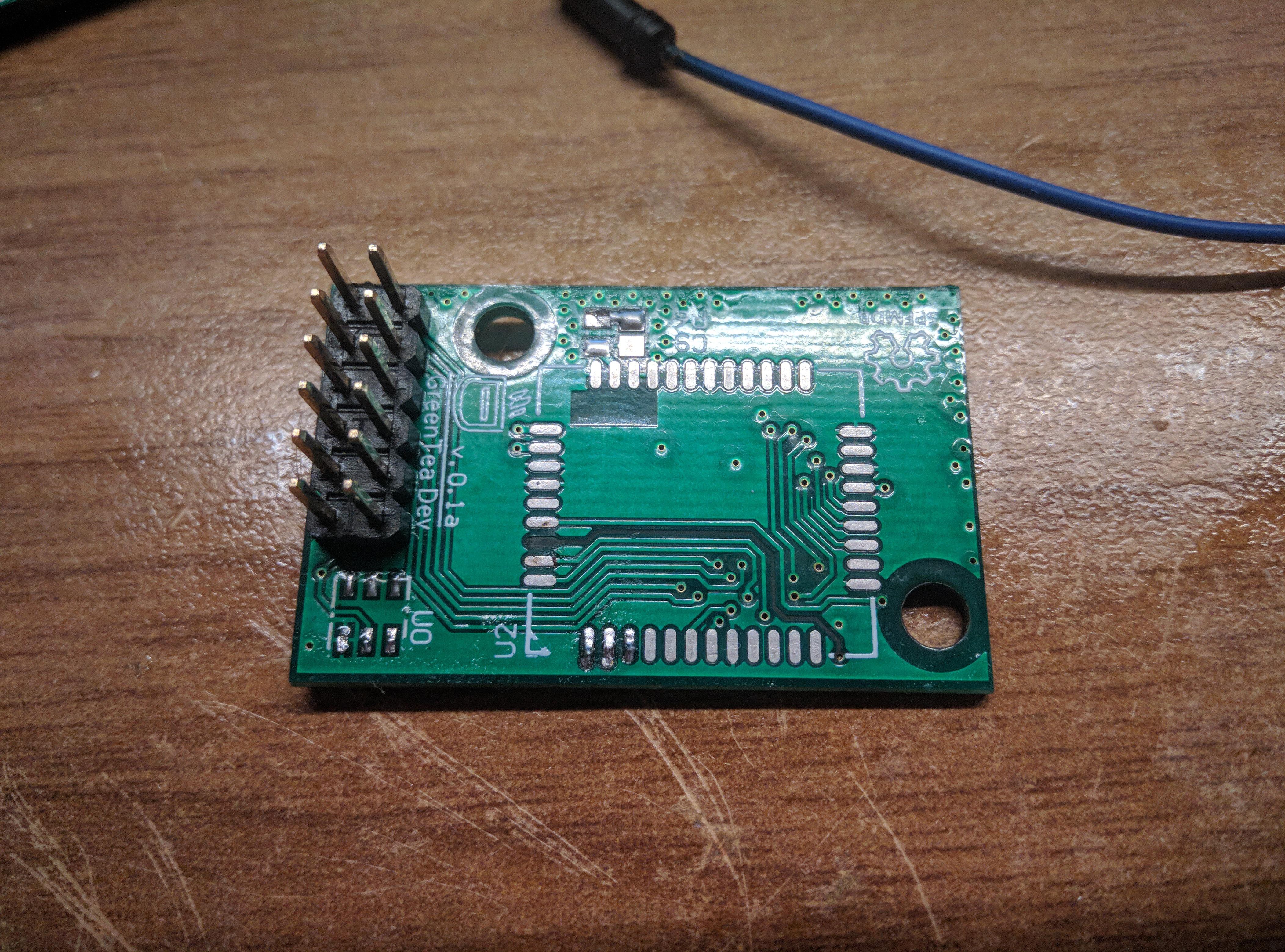
SIM800 Expansion board: The nightmare is over
08/02/2018 at 23:12 • 0 commentsI do not want to miss out on useless talk. (It's late and I want to go to sleep)
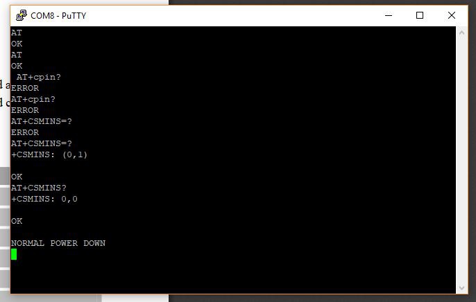
Today I received the new TXS0108E. I wanted to do some tests with these components. These, unlike the TXB0108, are designed for Push-Pull and Pull-Up applications. I wanted to try to understand if the problem was caused by some resistor inside the SIM800 module that created confusion with the direction auto detect of the TXB0108 IC.By doing some tests I noticed some improvements on the behavior with the TXS variant but the communication still wasn't working.
In desperation I opted for one last attempt (Before replacing the level shifter with a pair of mosfets on the design). I decided to replace my FTDI cable with an unpopulated ARDUINO board. I took the PWRKEY low for two seconds, I waited but I did not get the message "RDY" as wrote in the datasheet. I tried to write random characters but I did not get an answer. Fatality I did not know the baud of the module and the datasheet is not very clear (I have forgot since last test days). I then looked in the code of the "TinyGSM" library: to auto-boud probe the library tries to send "AT" and wait for an "OK" for reply.
Now disappointed I tried, getting as a result the notorious "OK".
![]()
Between one test and another I broke a PCB (it fell off and a track was torn off), and I changed the chip between the two models several times; comparing the serigraphy I found that the "test" working I had obtained with the "old" chip or the TXB0108!
![]()
Probably the module worked from the beginning but my FTDI adapter did something strange and made this stage of the development process a hell.
Next week the SIM socket and the last pieces for the Baseboard (Power module and MOVs) should be delivered.
This is the current serial testing setup (I use the RESET to pull the PWRKEY to LOW):
![]()
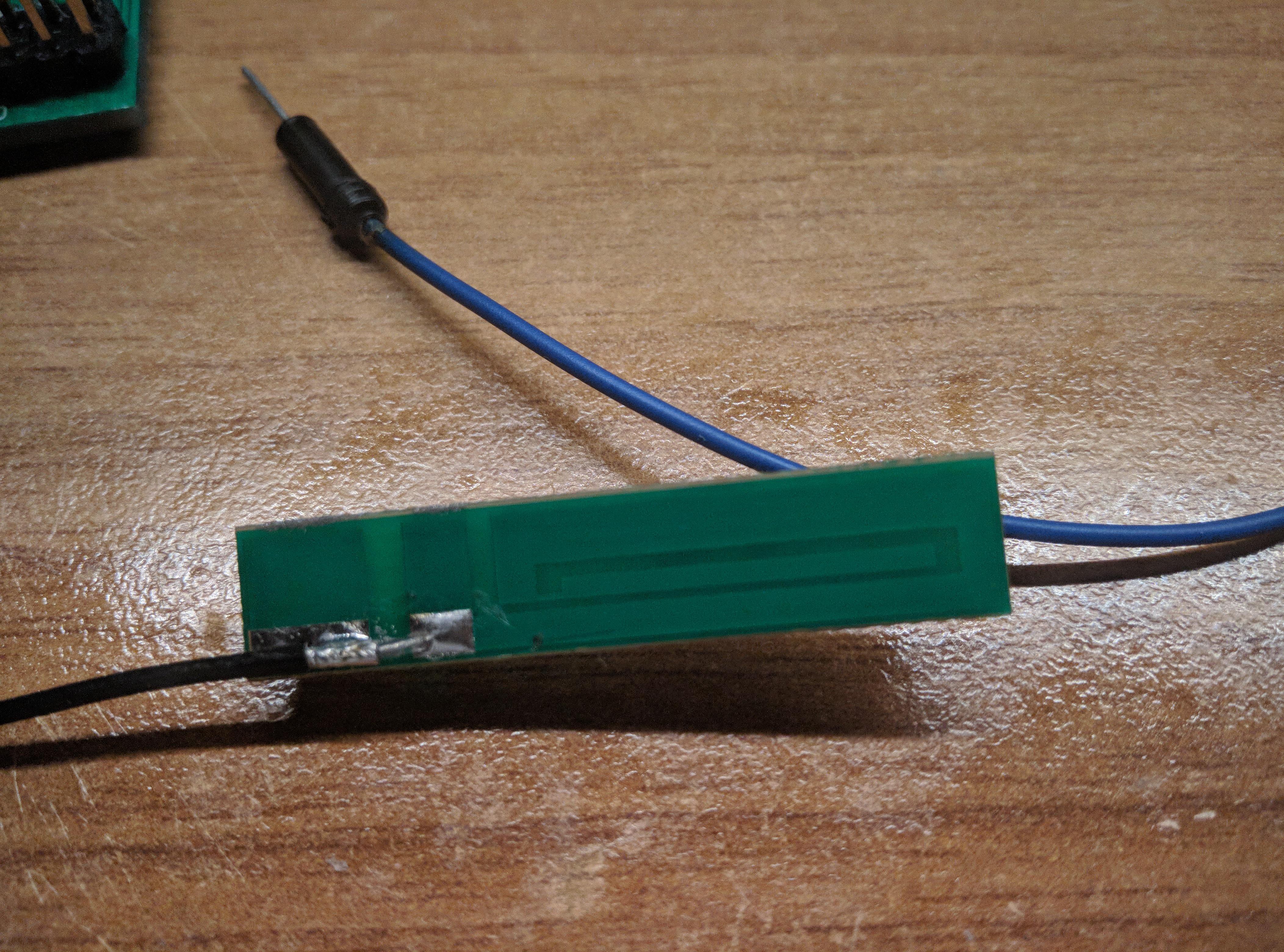
Just a quick note, I don't have fancy equipment to test things out but to me this desing look similar to a 2.4G antenna than to a GSM one. Any clue?
![]()
-
Learn 3D modeling
07/26/2018 at 14:01 • 0 comments
This project need a box to contain the electronic boards, I'm a IT guy and I have not experience on mecanical drawings, designing mecanical parts and 3d print. Hopefully my Univeristy allow me to have some professional products with an "educator" license. So using this method I decided to use Fusion 360. Back at school we studied a but of AutoCAD so working with parametric design is lot easier for me than other methods.
For test I have started to design the clips to hold the board in place, nothing fancy just two pieces one with a smooth border to guide the board in position:![]() After testing out the sketch and extrude functions I have started to make something more complex, This is my currect design for the box, using the analysis tools I have created a cut plane to see inside the box.
After testing out the sketch and extrude functions I have started to make something more complex, This is my currect design for the box, using the analysis tools I have created a cut plane to see inside the box.
The smaller board is the GSM module, the second one is the Baseboard. Both have been imported iinto fusion from the SETP file. (exported by Circuit Maker)
The third one is the fornt board but as you can see, the front board is not populated becouse I'm still designign that one. I want to be shure that the others works before starting the development of the ARM board.![]() The back lid is thinked to help the board staing in place and isolate the internal from a screwdriver. To protect the low voltage stuff on the front board I have added a plane to isolate the two.
The back lid is thinked to help the board staing in place and isolate the internal from a screwdriver. To protect the low voltage stuff on the front board I have added a plane to isolate the two.
This is the lateral view of the box, I have hidden all the unnecesssary stuff. In this way you can see how the back lid lock the board in position.Another
![]() Unfortunally i'm still thinking a way to lock the back lid and the isolation plane into position, I want it to be easily removable so I can add and swap modules easily.
Unfortunally i'm still thinking a way to lock the back lid and the isolation plane into position, I want it to be easily removable so I can add and swap modules easily.
The next picture shows all the layers stacked together.![]()
Unfortunatly things don't go always as planned; Even if I have added 1mm spacing the print is a bit smaller. The boards don't fit in without pushing it in with lots of force. The print also have lot's of warping.
Unfotunatly my friend don't have experience with ABS so we are tring and failing.![]() Another error is the design is the hole for the SIM tray. Unfortunatly the module can't be installed. So I will have to move the SIM groove to the back lid.
Another error is the design is the hole for the SIM tray. Unfortunatly the module can't be installed. So I will have to move the SIM groove to the back lid.![]()
On the main page you can find the render of this box! -
A step back: make the pcb
07/26/2018 at 10:16 • 0 commentsFor the pcb I choosed to a company that in the last period is papering the web of advertising!
The catchy price allowed me to make the panels, I had never made them. I used the excellent videos of EEVBLOG to learn. As a stencil would have helped me, I decided to order that too.
![]()
![]()
I'm certainly not an expert, the quality seems good, the only flaw I found is the thickness / quality of the solder mask. I noticed that it is easily scratched exposing the copper layer.
Even the silkscreen looks like quality and despite the very small font the result was excellent. (Only the "i" and "l" are too thin) This is a limit case: different components in a decidedly reduced space!
![]()
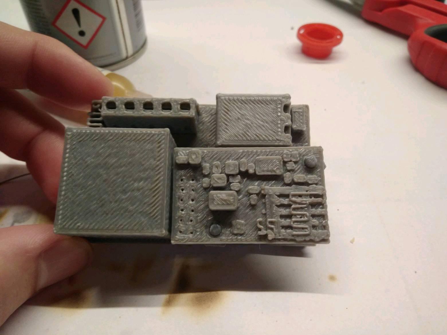
What to do while I was waiting the pcbs? Thanks to the STEP export function of Circuit Maker I was able to 3D print the pcbs and thest the physical dimensions of the boards. (I don't own a 3d printer so I had to ask a favour to a friend)
![]()
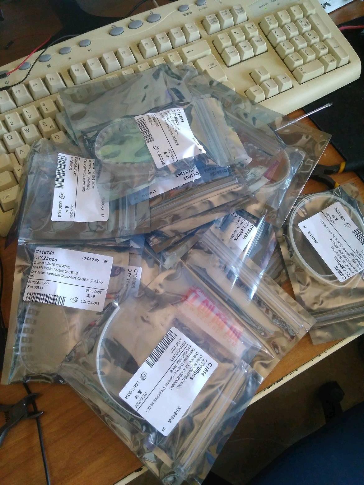
Fiew weeks later also the components that I had ordered arrived:
![]()
And the assembly and testing process started of the first prototype board.
-
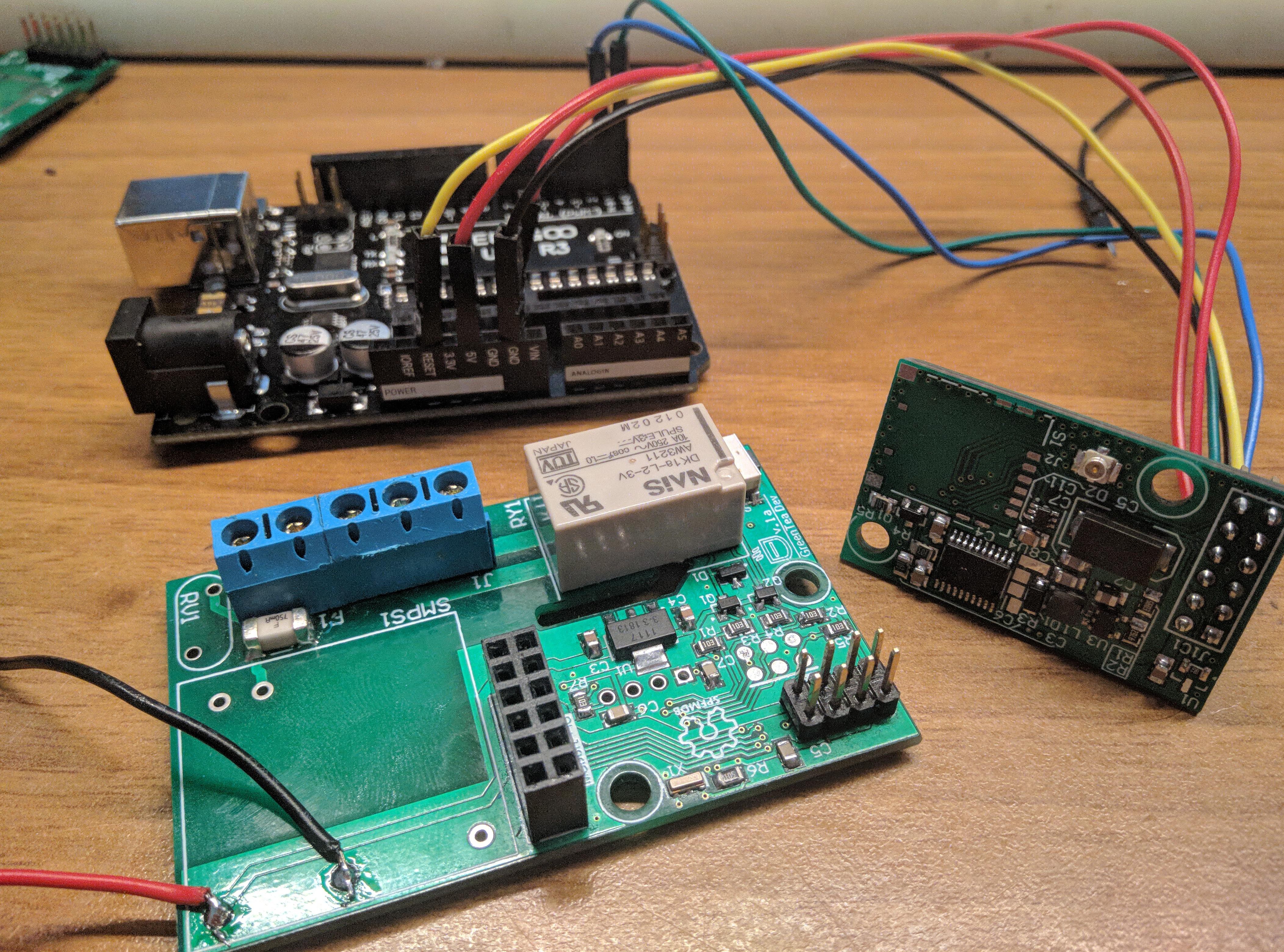
Testing out the baseboard
07/20/2018 at 15:18 • 0 commentsAs you have seen I had a huge problem with the SIM800 module. But the design of the basebord looks roock solid. Even if I have made a few mistakes.
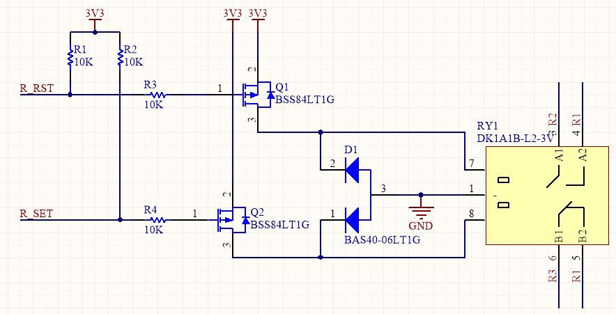
Thi is my first experience with mosfets, I never used before. (At school I only used opamps. Discrete semiconductors weren't on my school program)
I have spendt fiew time online looking at how a mosfet works, how to choose it. Due to the relay coil configuration I had to choose a P-Channel mosfet (BSS84L).
I was expecting something wrong, really wrong. I used a couple of times standard BJTs (using already made schematics) as on off switch but nothing more. I have soldered all the parts. I also mixed the diode and the mosfet trains so I had to rework my board.![]()
With the multimeter in my hand I measured the continuity, I checked for shorts and I have found one with the reset chip of the ATmega. At that time I tried to see if it was due to my 0-level skill on SMD soldering.
I tried to apply power to the board, just to see if the magic smoke would come out: nothing.
I then started the search process of that short-circuit the pullup was looking fine, so I decided to remove the microprocessor (There was nothing ele on that line). The short was gone! I may have fried the chip with a too high temperature. I than lowered it and soldered a new one. After that the reset line was HI so I was able to program the IC.I have soldered the ISP wires on the programming pads (I'm still working on the programming clamp) and using an Arduino Mega I burned the bootloader to the IC, I uploaded via serial the classic blink example.
I have no LED on pin 13 so I simply hooked the multimeter on the pin. It was working!Sorry I don't have any photo of this stage :(
The bootloader was working the microcontroller was running a sketch. The next step was to test out the relay part. I wrote a couple of lines inside a loop to toggle on and off the relay.
This is a bit more complicated than usual. This is a dual coil latching relay so I seed to generate two pulses to toggle the state.
I wrote the following code:// the loop function runs over and over again forever void loop() { pulse_relay_pin(RLY_SET_PIN); delay(5000); // wait for a second pulse_relay_pin(RLY_RST_PIN); delay(5000); // wait for a second } void pulse_relay_pin(byte pin) { digitalWrite(pin, HIGH); delay(100); // wait digitalWrite(pin, LOW); }The relay was toggling, but it was making an odd sound. Initially i was more concernd about the protection diode so I hooked up my DSO to see the voltage spikes. I then realized why the relay was making that odd sound. Have you spotted the error on my previous code?
I'm pulsing HIGH but the mosfet are P-type so they are "active LOW" (Yes I know that is not so simple), I figured this out becaouse the voltage across the diode was always 3.3V.
After correcting the code all was working fine:void setup() { pinMode(RLY_RST_PIN, OUTPUT); pinMode(RLY_SET_PIN, OUTPUT); digitalWrite(RLY_RST_PIN, HIGH); digitalWrite(RLY_SET_PIN, HIGH); } void loop() { // Same as before } void pulse_relay_pin(byte pin) { digitalWrite(pin, LOW); delay(100); // wait digitalWrite(pin, HIGH); }I left the board running for half a day while I was tring to troubleshooting the SIM800 and after all that time it was still working. Not a complete durability test but at least I have some hope.
I'm still waiting for the PSU, but i'm running the board with 5V via the on board regulator. Looks fine, it is cold under the load of the relay and the uC.
![]()
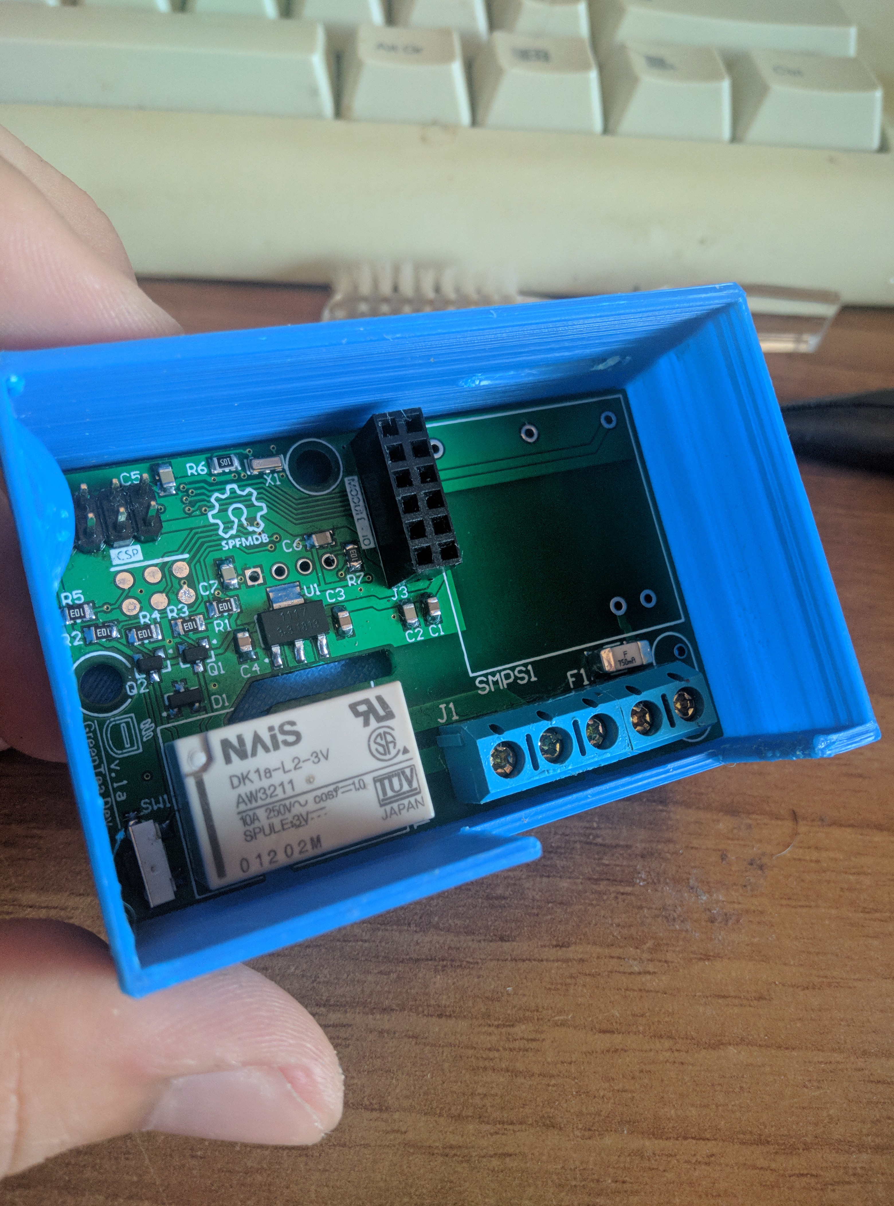
The baseboard, the SMPS is still missing :( -
SIM800 Expansion board: Where the nightmare begin!
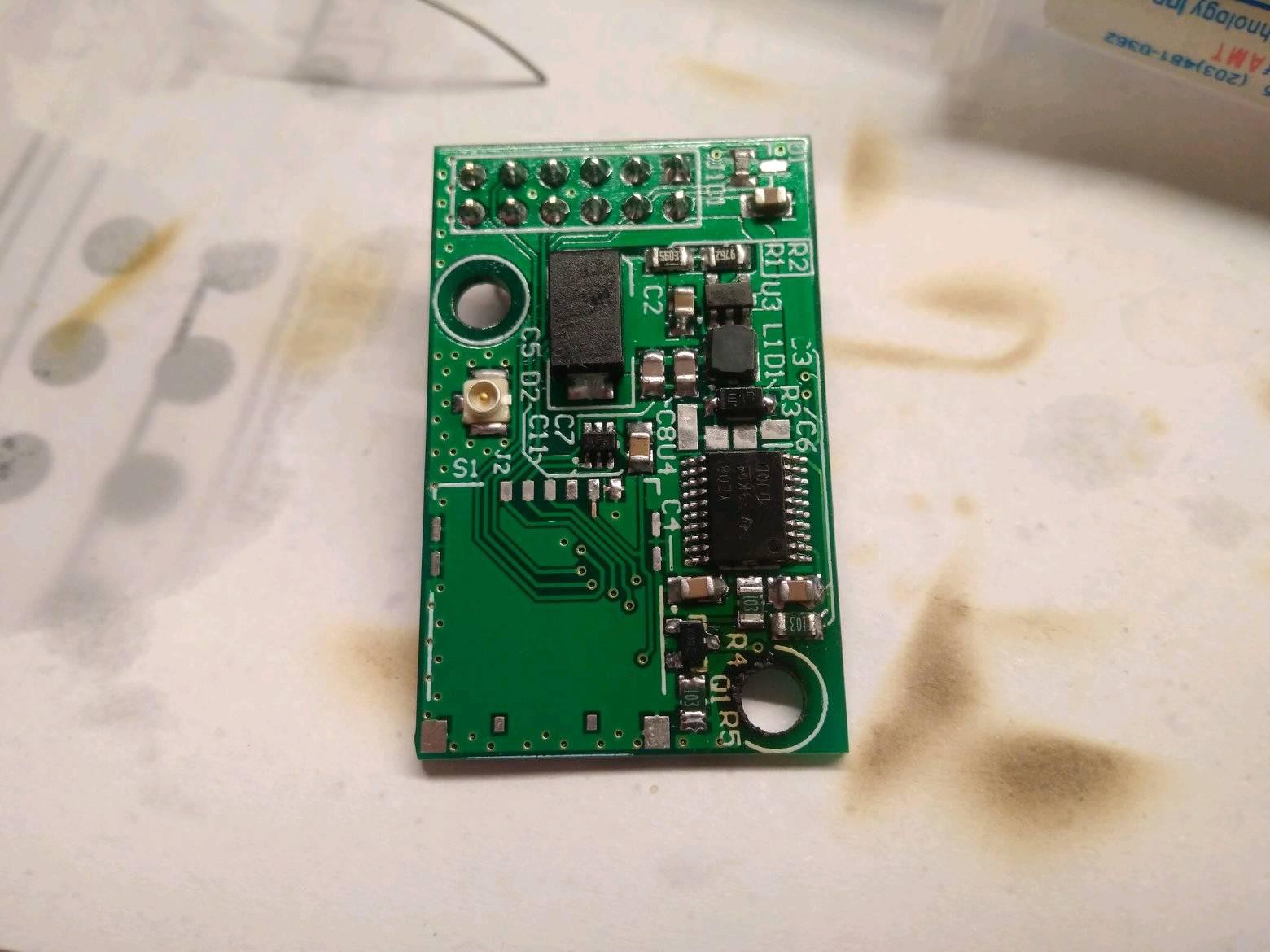
07/17/2018 at 09:17 • 1 commentTo add the GSM / GPRS I opted for the SIM800C chip (The one witch castelled mounting holes) , it is small and does not cost much and it sends SMS. It could also call, but when I designed this module, I still did not know where I was going with the project.
![]()
First of all it should be said that a regulator is integrated in the SoC used inside these modules (it is designed for battery-powered cellphone). The module must therefore be powered at a voltage of 4V. Could not they make everything simpler? Having 5V from the switcing power supply I would have a fall of around one volt. Chinese manufacturers use diodes (with poor success), so I have opted for a switching regulator.
For the purpose I choosed a TI TLV62569, small footprint (The board is 35mmX24mm) and needs few external components.
Having never used a regulator of this type (I am self-taught) I read multiple times the datasheet, some things unfortunately I wasn't abe to understand properly. Despite this I made the circuit, the fact that the module in transmission can use up to 2A still worries me. (I don't have a load tester)Using the documentation found online I started doing the schematic for the SIM, a condenser here, one there for the bypass, one zener, and the ESD protection diodes for the SIM.
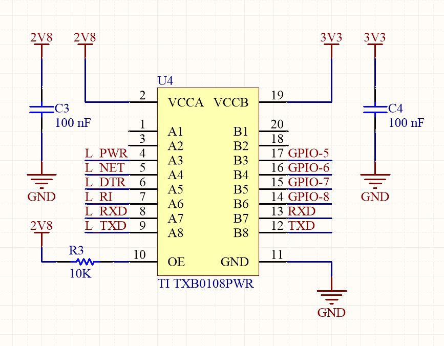
The development seemed to spin smooth, but at some point, I was reading the "UART Communication" section of the hardware design of the SIM800: The I/O is at a voltage lower than 3.3V, damn!I then started looking through the components drawers to see if I still had logical translators of an old project ... fortunately I still had many. This is the TI TXB0108PWR. (I had used these for the same purpose in my project of the car controlled via the internet. The model had an ArduIMU board with sensors and worked at 5V and the raspberry instead has a 3.3V IO.)
This is commonly used for the same needs I have so I decided to use that on my design. And here is where the nightmare started: Back on by RCWeb Car i had similar problems but I solved it by buing chips from a official distributor instead of ebay. But this time it don't worlk even if I use the "original" chip. The schematic looks ok to me. There are the two bypass caps on the voltage rail A and B, the enable pull-up resistor but for some odd reason if I apply a square wave on one side this is not present on the other.
I tried to load that pin using a resistor divider but also in that case I got a stuck HI output on a voltage level different from both sides A or B. I also tried with pull-up and pull-down resistor and tried to measure the values on the other side but if I change the logic state the "output" is locked on a mid value below the side A supply rail. This happens also on the reverse. I think that this have something to do with the auto detect direction system that the chip have.![]()
Unfotunatly after two days of attempt I'm not able to make this IC working. If you have suggestions you'r welcome to join the discussion!
FCThermostat: Another overengeneered IOT device
A new way of thinking to a IOT thermostat:


 After testing out the sketch and extrude functions I have started to make something more complex, This is my currect design for the box, using the analysis tools I have created a cut plane to see inside the box.
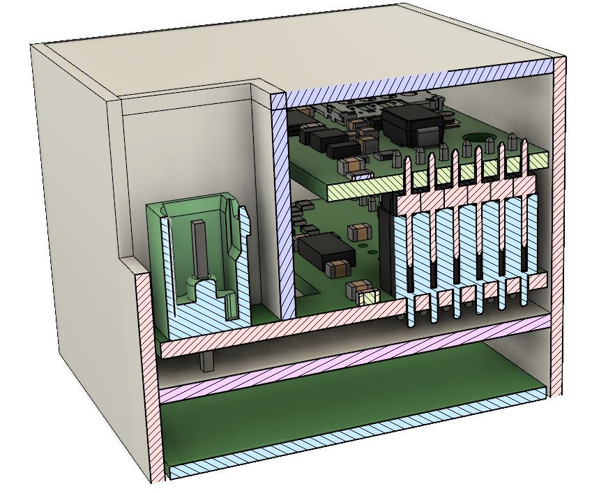 The back lid is thinked to help the board staing in place and isolate the internal from a screwdriver. To protect the low voltage stuff on the front board I have added a plane to isolate the two.
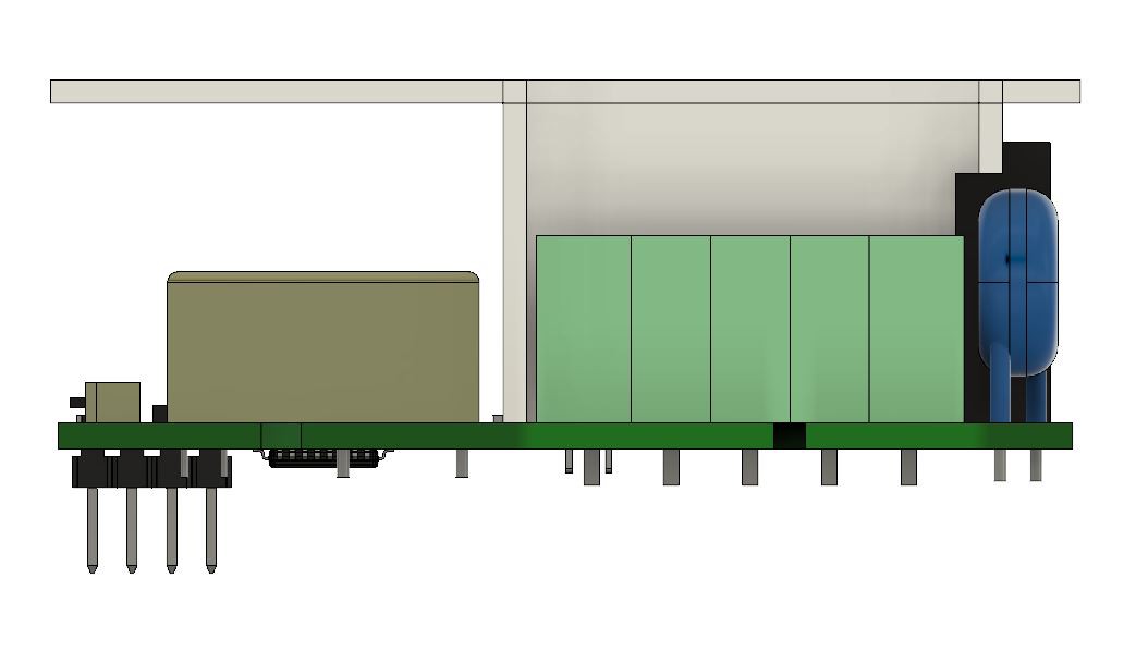 Unfortunally i'm still thinking a way to lock the back lid and the isolation plane into position, I want it to be easily removable so I can add and swap modules easily.
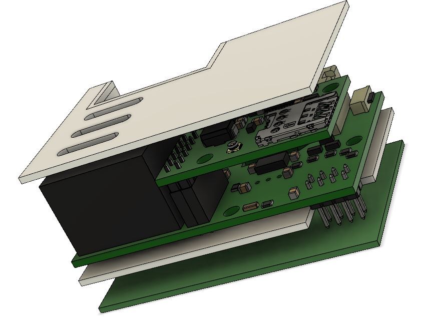
 Another error is the design is the hole for the SIM tray. Unfortunatly the module can't be installed. So I will have to move the SIM groove to the back lid.