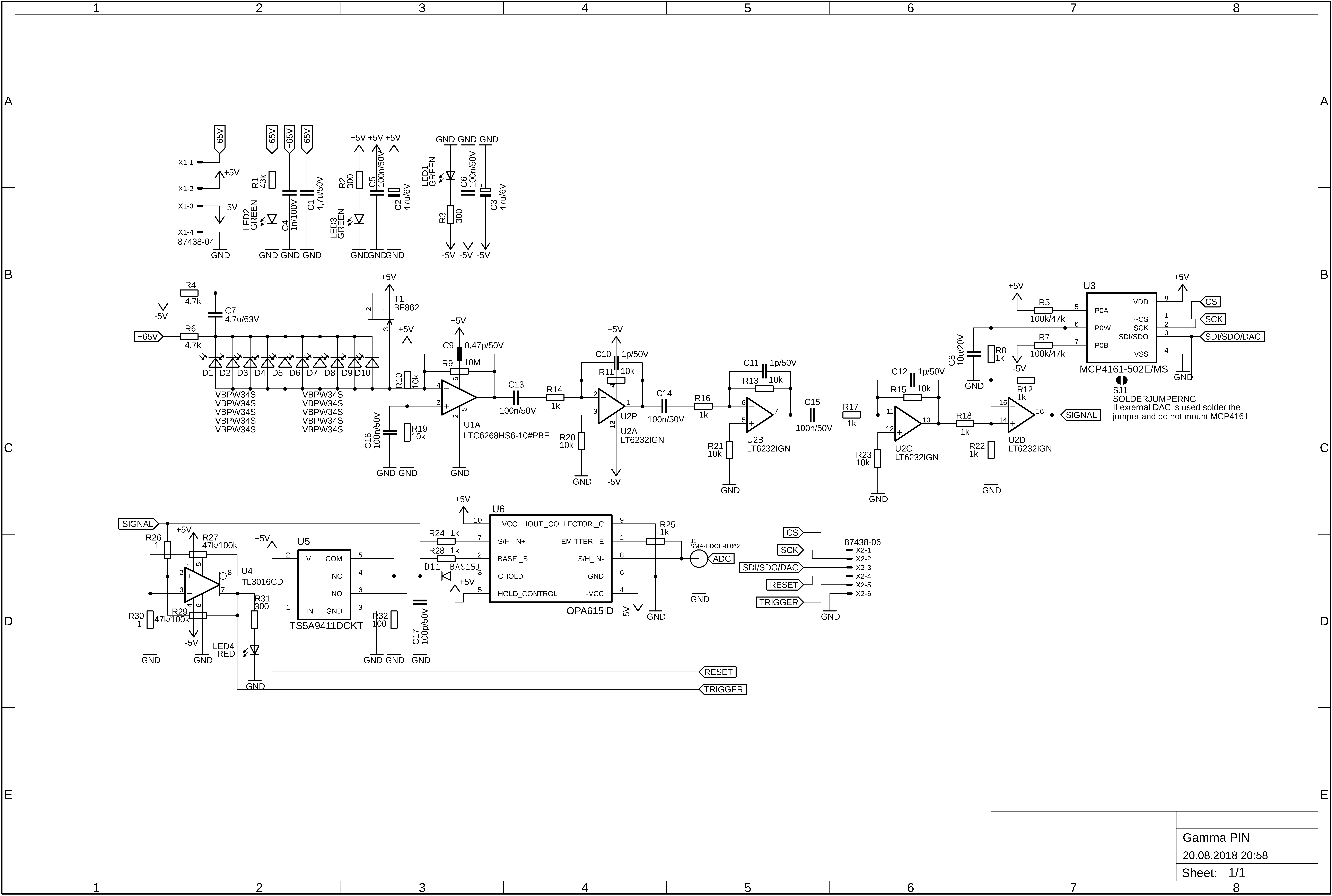
After two weeks of designing the PCB and optimizing all the routes I finally managed to send the Gerber files to manufacture. As previously mentioned I wanted the board to be in a shape of a thin stripe, so the result is board with all components on one side having dimensions of 160x11mm. Whole design is with regard to parasitic capacitances, that should be minimalized to allow the best performance.
The detecting "stripes" may later be aligned to form a multi-layer matrix to perform some particle trajectory or coincidence research. I have aimed to make it quite universal so there is a dashed line where the board may be cut to solder the photodiode in right angle. There is also an option to bypass the MCP4161 by connection its 2nd and 6th pad which are in a straight line and use external DAC to set the noise cancelling level.


I ordered 50 boards from the JLCPCB, so if you want to test this design contact me and I may sell some to you. The schematic includes all the blocks mentioned in the description and some additional capacitors for filtering the power lines. The power stabilizers and IC are to be located on external board from which all the stripe detectors will be powered all together.

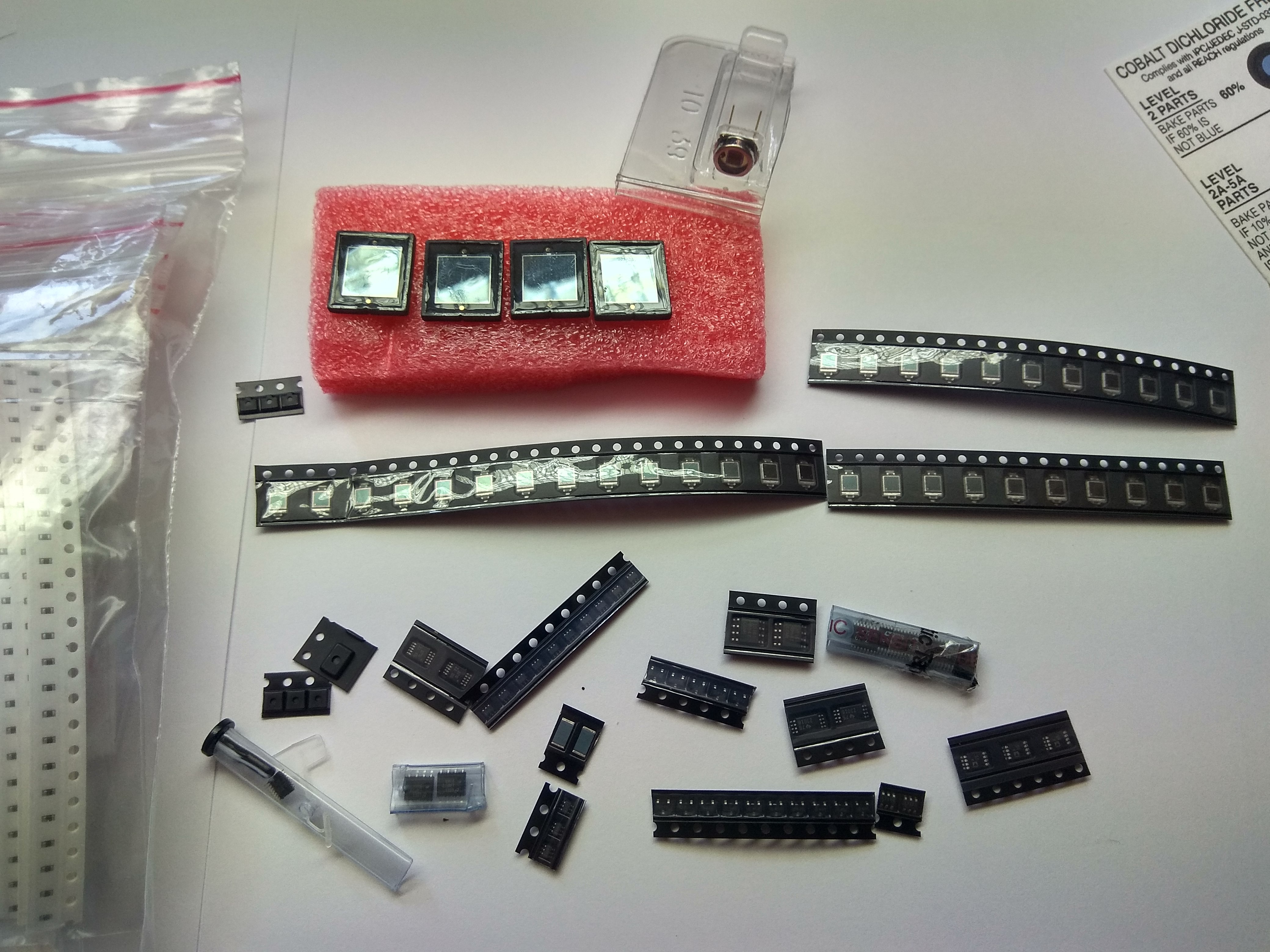
In a few days’ time when I get the boards I shall begin assembling the detector stage by stage to test it all. I have acquired all the necessary parts and am ready to proceed to the next stage.

Discussions
Become a Hackaday.io Member
Create an account to leave a comment. Already have an account? Log In.