The first prototype is quite fine but it has some errors that I noticed during the assembly and testing. The detector will be still developed. I hope that the second version will be satisfactory enough to meet the requirements for the first spectroscopy. During the tests I became acquainted with the STM32 ADC and DAC. The detector is so sensitive that uploading the program to the development board caused oscillations. Having noticed this to prevent additional digital noise I decided to use non-volatile programmable potentiometer. Once the value on the MCP4161 is set. It will be disconnected to except any distortions from the signal busses. I am currently working with NUCLEO-H743ZI but after the prototyping is finished the detector should run with a “Blue Pill” board featuring STM32F103C8 microprocessor that should handle everything easily.
Things to improve:
The signal processing
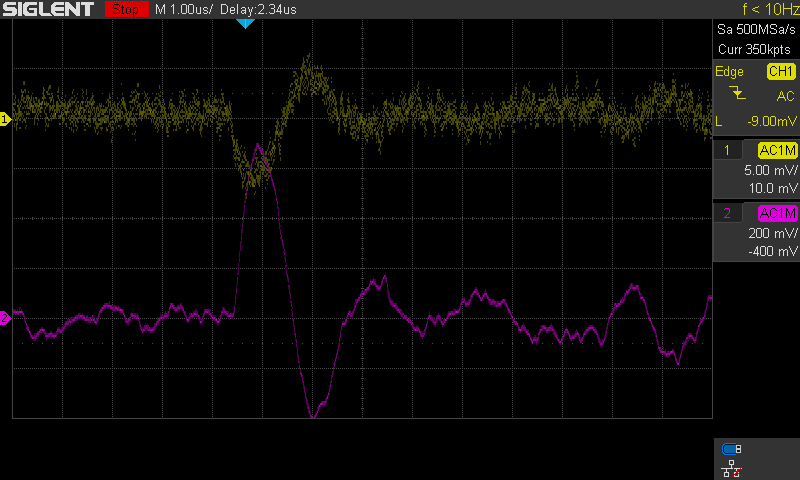
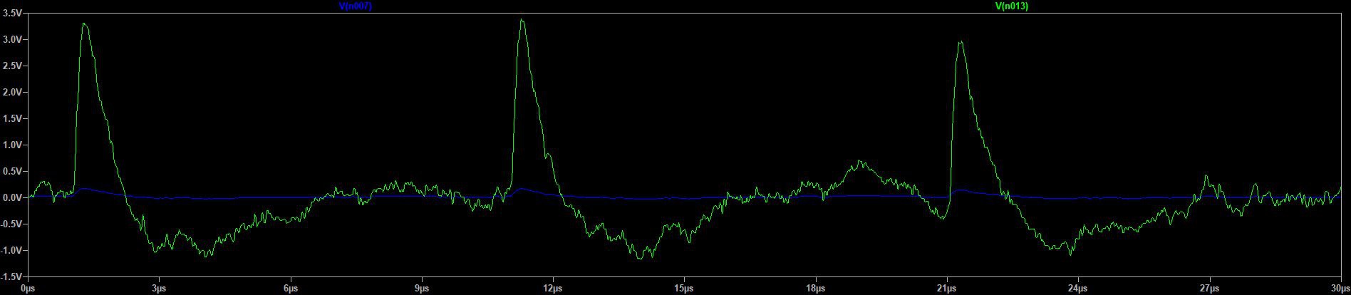
- In the first version the pulse from TIA is simply amplified three times and then "lowered" so that only the meaningful peaks are positive. Then they are acquired by the ADC. Apart from the desired signal, the noise is also amplified. It results in distorted and spiky pulse with very short peaking time, blurred amplitude and unnecessary restriction of op-amp amplitude range. The capacitive coupling of the inverting amplifiers also causes massive undershoot and tail oscillations, that disturb the baseline and amplitude of the following pulse.
![]()
Signal after amplification with visible distorted peak ![]()
Signal after amplification with visible tail oscillation - baseline fluctuation - To avoid the pulse distortion the noise floor should be removed first and then the resulting peak should be shaped to resemble the gaussian function. It can be done by using 3-4 op amps just by changing the order of the processing. First there should be a subtractor that will "lower" the signal in order to make only the significant pulses negative. Then the signal is fed to an ideal negative rectifier based on another op amp. Finally, it's processed by double Sallen-Key filter which serves as Gaussian shaper. After these alterations the signal is connected to the acquiring segment by a single decoupling capacitor so that its normal level is around 0V.
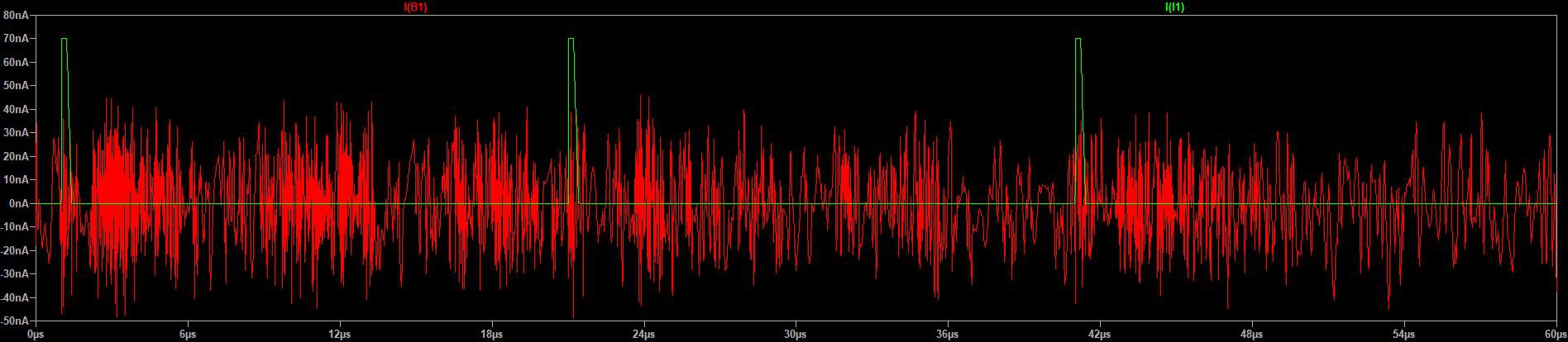
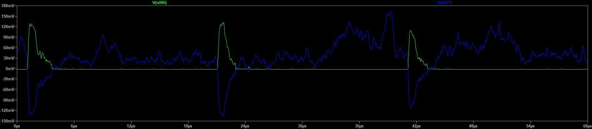
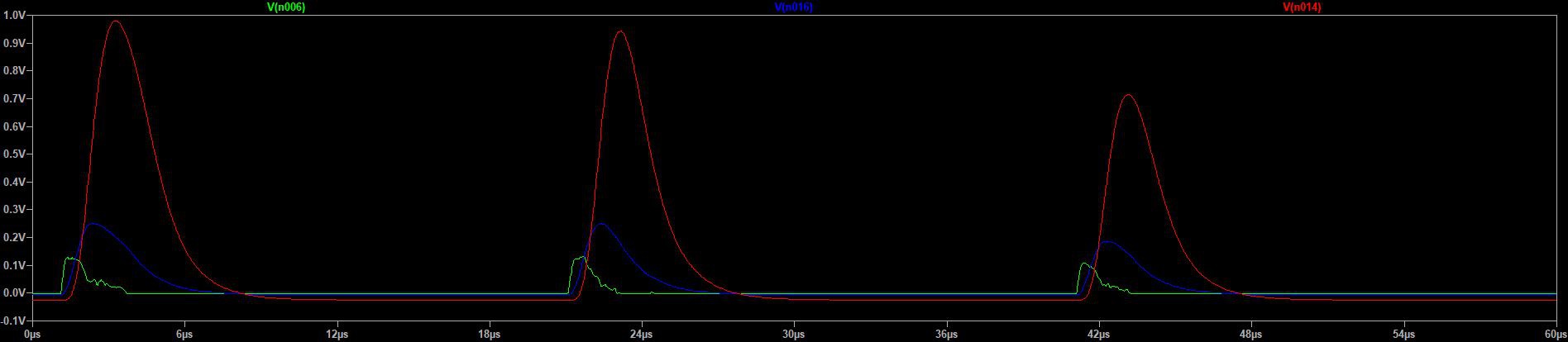
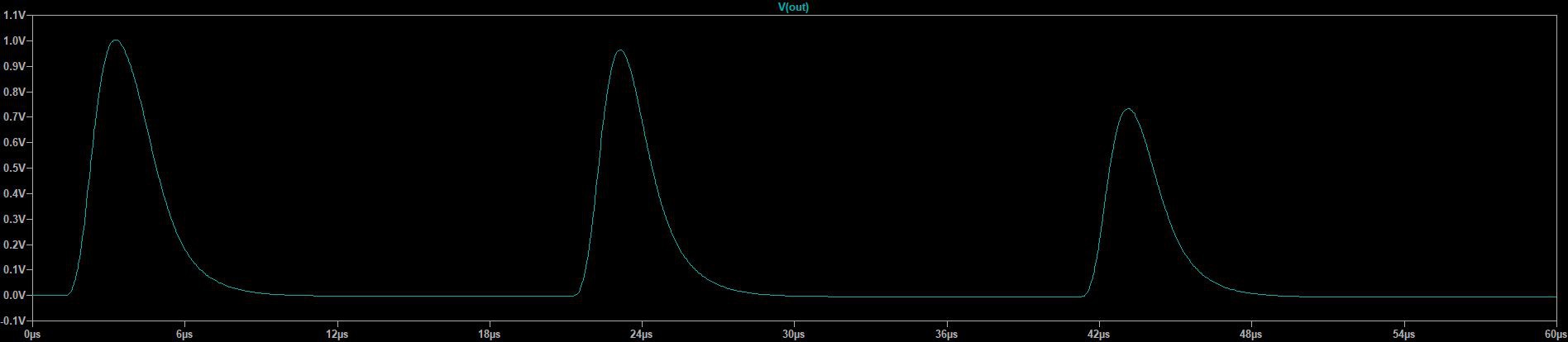
- The simulations with the described above configuration nicely visualize the signal processing. To improve accuracy in the LTspice model I added a white noise current source in parallel. It should resemble the thermal noise of the semiconducting PIN diode.
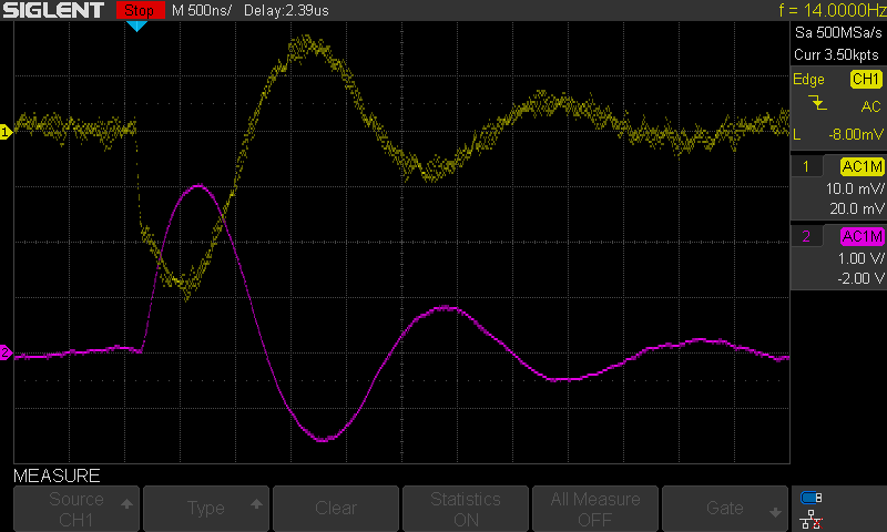
Old version simulations with noise
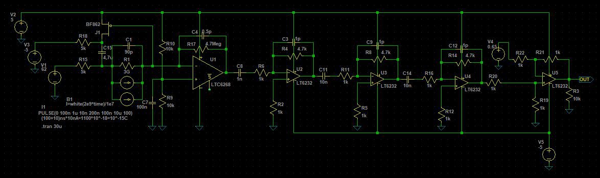
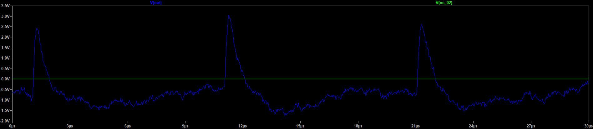
New version configuration
Supply filtering
- Fast, wide bandwidth op amps and comparators generate interference that unfortunately excites more sensitive parts. The whole detector is extremely sensitive to any change of charge. The additional pulses generated by switching caused it to oscillate. At first, I thought this was caused by the high integration of the board and crosstalk. But in the end, it turned out to be just lack of decoupling capacitors, that easily prevent the excitation. The few capacitors placed at the distant end of the board were not enough.
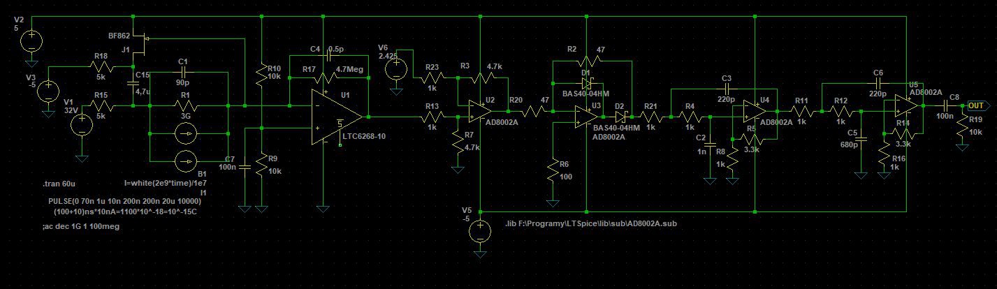
- To solve these instability issues, every integrated circuit supply node will be powered through a 100 ohm resistor with two capacitors attached. One ceramic 100nF and one tantalum 4,7-22uF placed as close to the pins as possible. It may seem overengineered but it is neither an expense nor it would have saved lots of space on the board.
![]()
Set of capacitors, each connected to its own IC
- To solve these instability issues, every integrated circuit supply node will be powered through a 100 ohm resistor with two capacitors attached. One ceramic 100nF and one tantalum 4,7-22uF placed as close to the pins as possible. It may seem overengineered but it is neither an expense nor it would have saved lots of space on the board.

Compatibility
- My aim is to make this detector an accessible tool to measure and analyses radiation. Therefore, I have decided to switch from quad op amps to dual ones in MSOP-8 (V2 will include AD8002) package (with common AD pinout). It will enable a wider range of cheap replacements that will be later suggested for any widespread distribution or testing. There will be also an extended solder pad to mount the TEMD photodiodes too. The long array will have a V-cut at the end so that it could be snapped to install bigger detecting diodes horizontally closer to the TIA stage.
The case of undershoot and baseline restoration is still open and it will be verified whether the removal of the coupling capacitors and inverting amplifiers has solved the issue. If not, there are some proposed solutions in the nuclear research papers. Another thing to consider is addition of pile up rejection circuit and coincidence detector.
Discussions
Become a Hackaday.io Member
Create an account to leave a comment. Already have an account? Log In.