 H00GiE
New Design
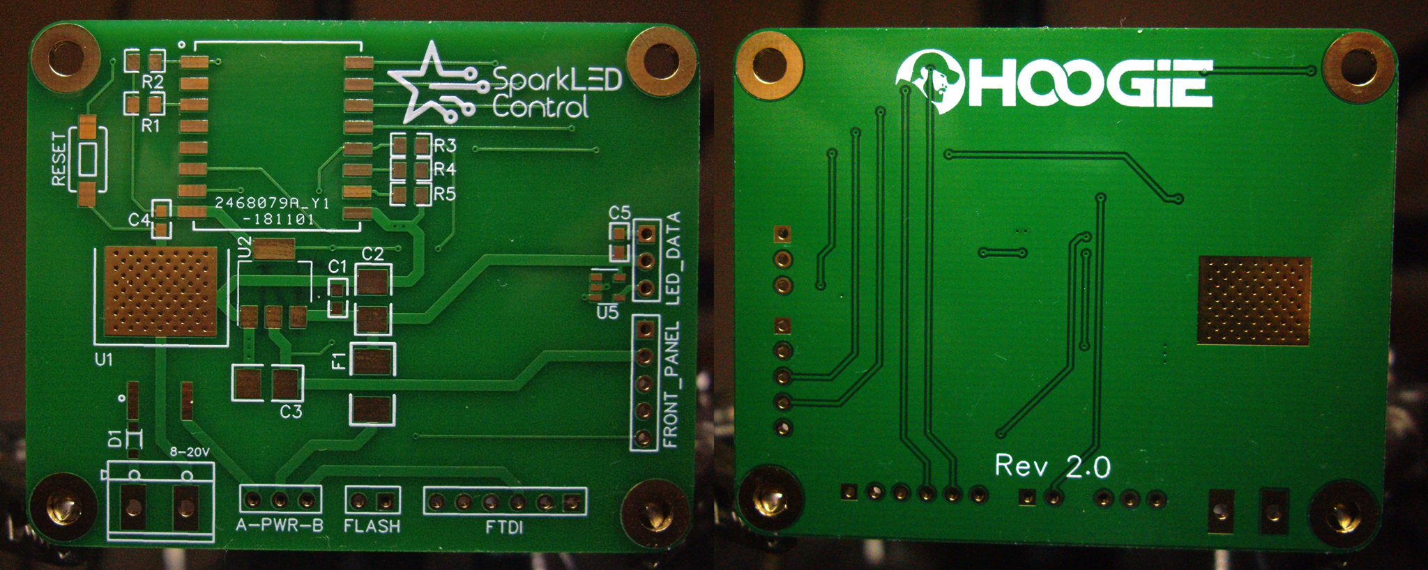
The new boards (HW v2.0) were redesigned due to new cabling for the front panel.
(everything is I²C now)
New material
The new PCB is made with ENIG, a type of surface plating used for printed circuit boards. It consists of an electroless nickel plating covered with a thin layer of immersion gold, which protects the nickel from oxidation.
ENIG has several advantages over more conventional (and cheaper) surface platings such as HASL (solder), including excellent surface planarity (particularly helpful for PCBs with large BGA packages), good oxidation resistance, and usability for untreated contact surfaces such as membrane switches and contact points.
Discussions
Become a Hackaday.io Member
Create an account to leave a comment. Already have an account? Log In.