The Falstad simulation of the full adder has two parts. The first part creates the input signals for the adder:
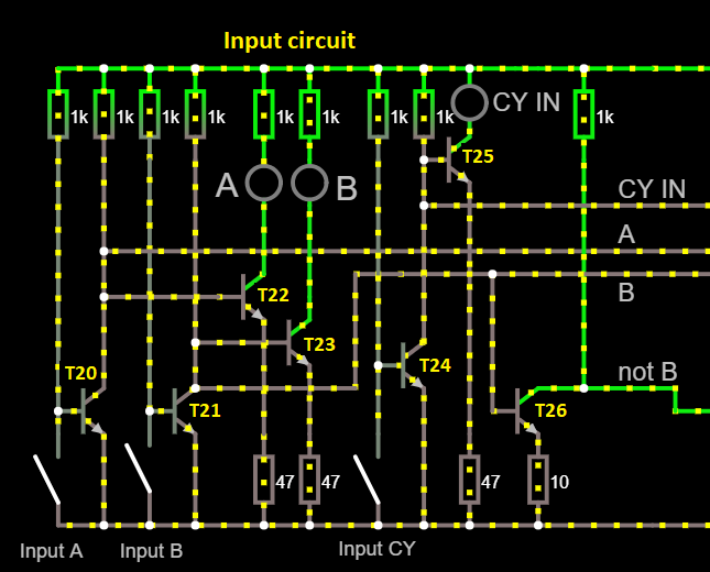
There are switches to change the input signals A and B, and the Carry input signal. There are also 3 LED's to check the input values. At the right side you see the 3 created signals CY-IN, A and B, and an inverted version from B.
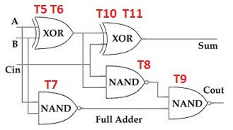
The second part is the actual adder:

This is actually an implementation of a classic adder design. The following picture shows the function of the transistors:
Discussions
Become a Hackaday.io Member
Create an account to leave a comment. Already have an account? Log In.