 Jasper Sikken
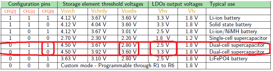
In revision 2 the PCBA was pre-configured to output 3.3V and 1.8V on the HV and LV outputs and these levels could not be adjusted. Now in Revision 3 you can lower the HV output to 2.5V using a solder jumper. When R4 is placed the HV output is 3.3V. When R3 is placed the HV output is 2.5V
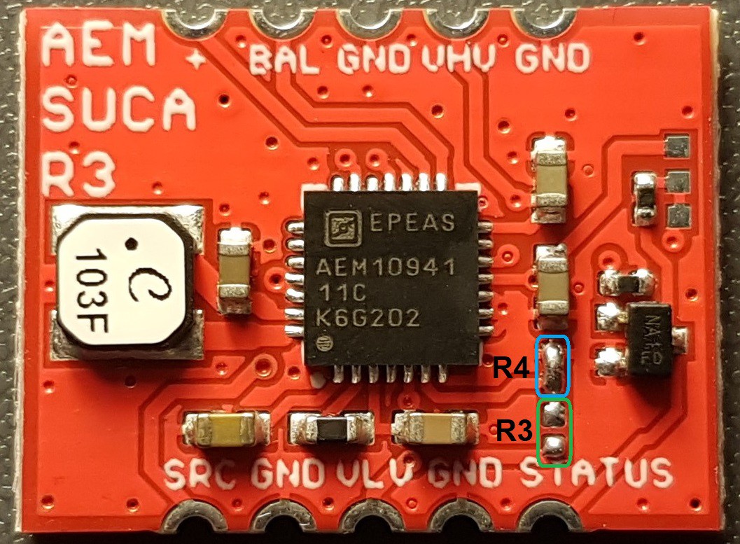
In my board R3 and R4 define CFG[0] is 1 or 0, see the table below (from E-peas AEM10941 datasheet)
Discussions
Become a Hackaday.io Member
Create an account to leave a comment. Already have an account? Log In.