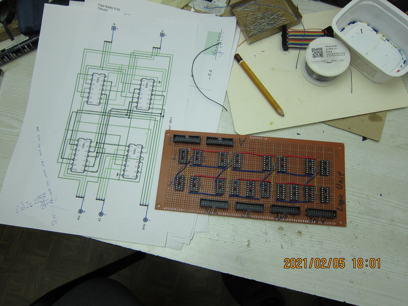
While soldering adders and logic unit, I took a harder look at the overall ALU schematic, and also on the instruction encoding for its operation. I seemed to me that some changes there will be despite me being certain that the design is rock-solid.
The changes to the structure will not be very big though, just a couple connections moved. As for instructions, I think there shouldn't be instructions of type A <-- op(A,B), as they are totally redundant when there are A <-- op(B,C) ones exist. Thus some instructions words become available, but to utilise them decoding logic should become more complex.
As for the other parts -- I am thinking about redoing memory subsystem from scratch, as the one in the model right now became too irregular, as it seems to me.
On the hardware front, right now work is going on soldering the Logic Operations board, which will output results of bitwise AND, OR, XOR and INV operations from its inputs:

 Pavel
Pavel
Discussions
Become a Hackaday.io Member
Create an account to leave a comment. Already have an account? Log In.