 mitchell.dokken
I got the boards in about a week and a half ago. Nice job JLC pcb. I noticed a few things right off the bat:
- The TQFP-48 footprints are precisely the same size as the pins, which makes soldering and alignment really hard. I haven't been able to successfully do solder one yet, so I'll redo that part design for the next board.
- Using surface mount pads to mount the SBC is a bad idea. Its not easy to solder the further back rows. It should be through hole.
- Didn't measure inrush current before I designed the board, and this killed my DC-DC boost converter, and battery management ICs.
- Footprint for SI4720 RF transceiver is wrong. Its just wrong. I'm thinking of switching to discrete TX and RX ICs.
- Through hole design for the potentiometers is just wrong.
- Mounting screws for nanopi neo are off by about .1mm. Can't fully tighten the screws.
- I completely inverted the pinout of the neo, and now it is installed upside-down. As in, the CPU and RAM are facing downwards towards the main pcb. This is the opposite of what I wanted, and I need to completely redo it.
- The kindle battery mounts are slightly off, but they still work. Fit an M2.5 screw.
On top of that, the supplier of the CM6206 is moving their entire warehouse from CA to TX. It took over a month to get my 5 chips. In a huge 200 tray.
In the interim, I built the PCM2906 audio card and the FE1.1s USB hub projects for the square inch competition, and they both work! I've been thinking that the PCM290x would be better suited for this project, as it takes up a lot less space than the CM6206 design. I'll have to verify that on my next board revision.
To solve the whole "blowing up my DC-DC conv and battery IC" problem, I had to get back to basics. Using the relevant application notes from ON Semiconductor, I was able to experimentally get a design that worked for me. I have a lot of parts on hand, so I used an IRF7404 P channel mosfet and an AO3400 N channel mosfet.

I tested it on a 5 ohm, 100uF load. I used a simple button to enable Q1, with a 10k pulldown so its default state was off. After a few tries of swapping out parts, I got a pleasant curve that wouldn't break the electronic bank. 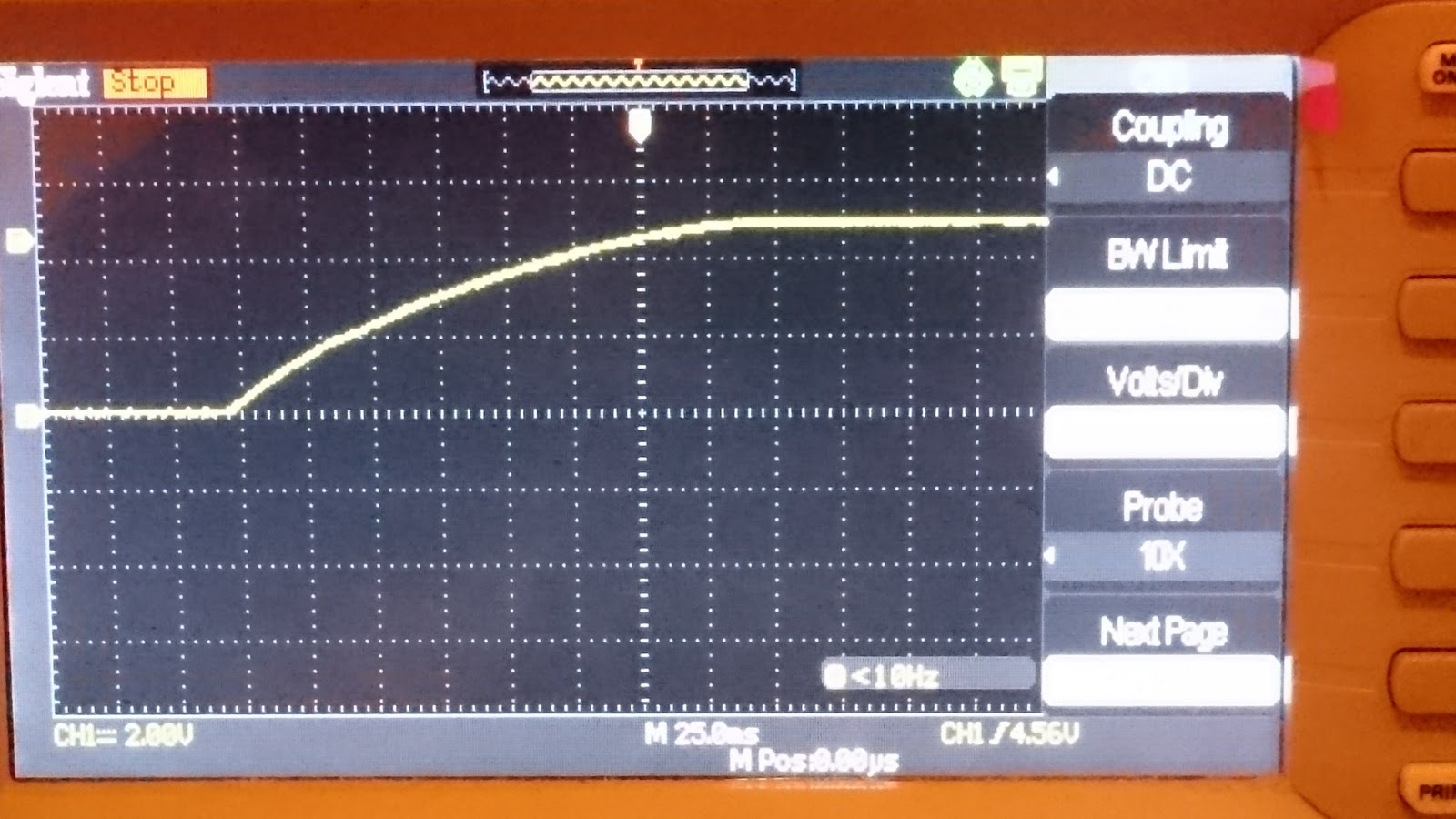
I finally installed the circuit on some spare room on the PCB, and everything worked!
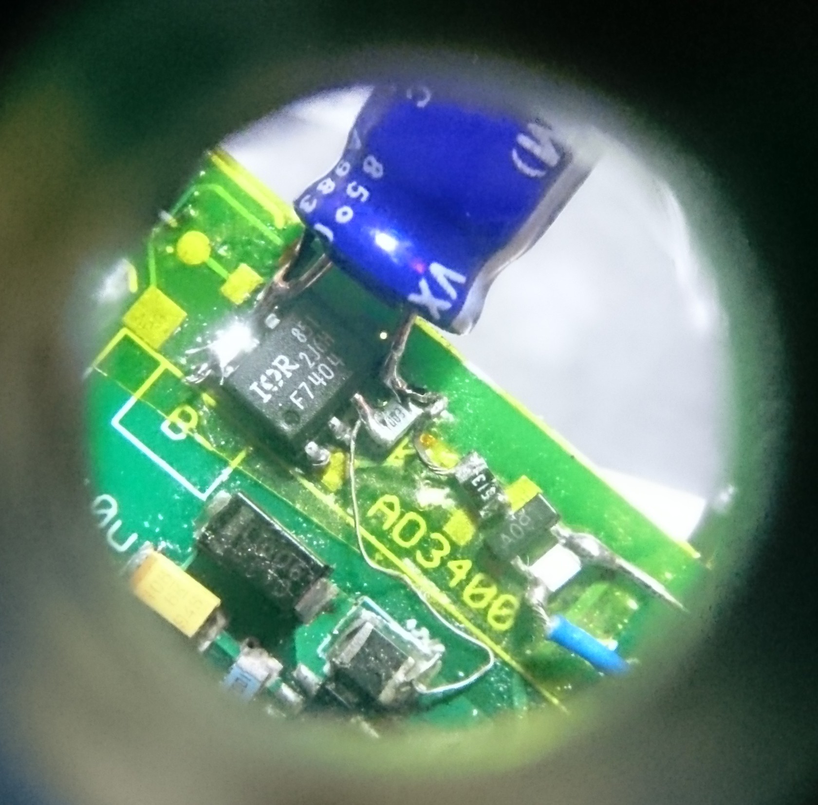
Had to use an eye loop to get this. You can see the unfortunate capacitor choice. I'll have to find SMD electrolytic variants. The ceramic and tantalum ones I tried didn't give the desired results.
During all of this, I also learned that the nanopi neo can run at 3.3 volts. As in, the 5v rail is only supplied 3.3 volts. I logged in and ran stress -c 4 for a while, and it never crashed. In this light, I've decided to forgo the main 5.1 volt DC-DC converter altogether, and use a smaller, accessory only 5v boost circuit based on the MT3806. I bought 40 of them for about 4 dollars shipped on Aliexpress.
This only complicates matters, though. I need 5 volts for USB accessories, but I also need a clean 5v line, using an LDO and ~6.5 volts from an MT3806 circuit. I also need a clean 3v3 line for the STM32, and a 3v3 line for any other accessories, such as the USB WLAN card. I measured it drawing upwards of 250ma in bursts during brief testing.
Anyway, I have the kindle battery working, the battery mgmt IC doing its business, a soft-start switch, and thats good enough for board 1. I'm going to make another board and get it here a week or two before the competition ends and prove the concept.
Thanks for reading!
Discussions
Become a Hackaday.io Member
Create an account to leave a comment. Already have an account? Log In.