 Gee Bartlett
I want to share as much of the design process i went through to get to a finished board.
I like to try and get stuff down onto paper really early on in the design process, for me it is important to get a good feel of what i want to achieve and sometimes it is even handy to go back to when feature creep come wandering in.
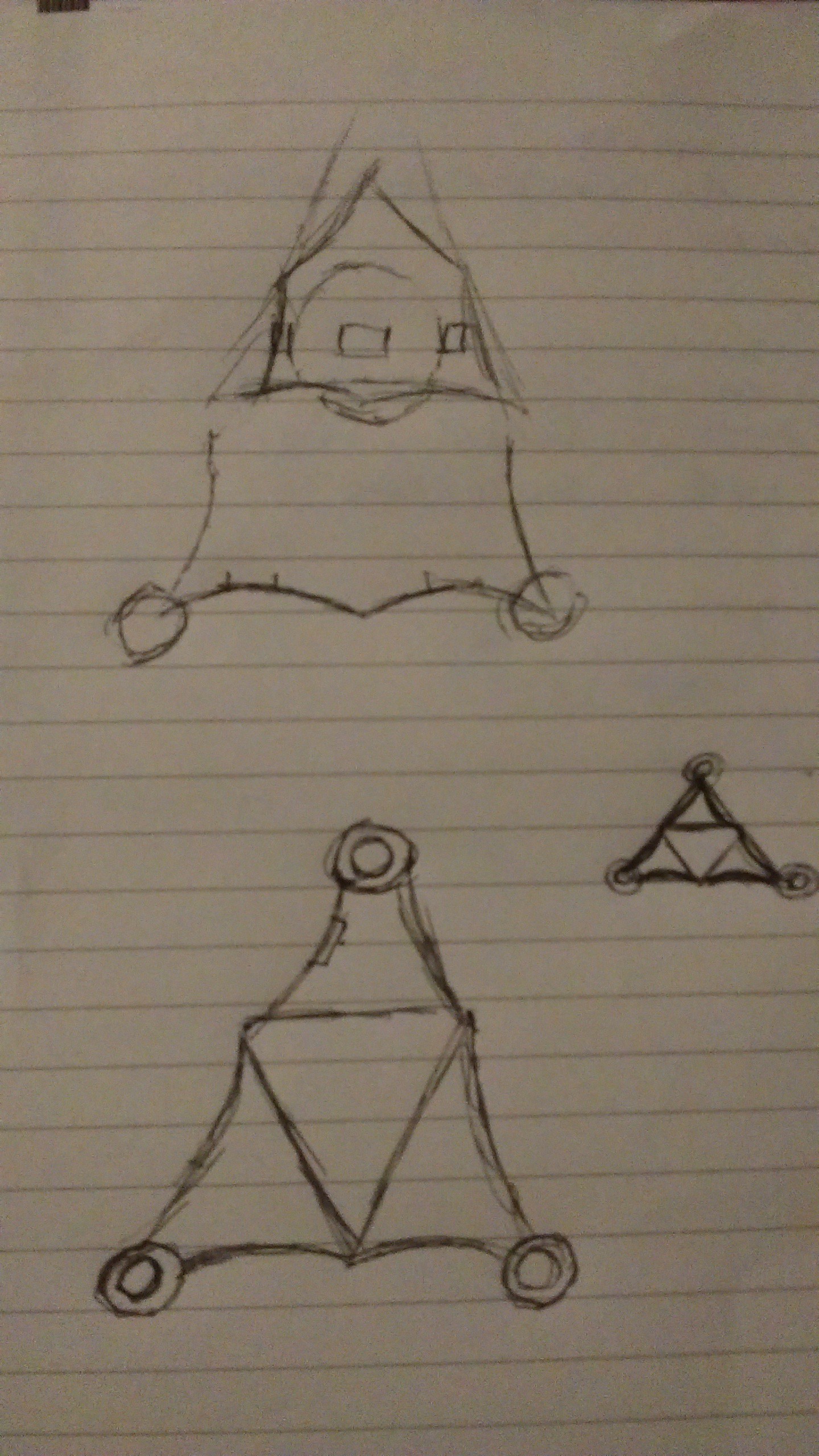
Having an overall triangular shape was important, It would help to make interesting shapes and patterns when the units are placed close to each other. Also note the rings on each corner for the sew-able connections . Also to note is my early attempts to fit a CR2032 coin cell holder as much i looked the battery dominated the rear for the PCB and left no room for the IR send and receive in the lower edge of the board, which is what lead me to eventually drop it .
Once I got rid of the battery holder the board became far more compact and it allowed me to consider the IR LED positions and how the units would communicate with each other.
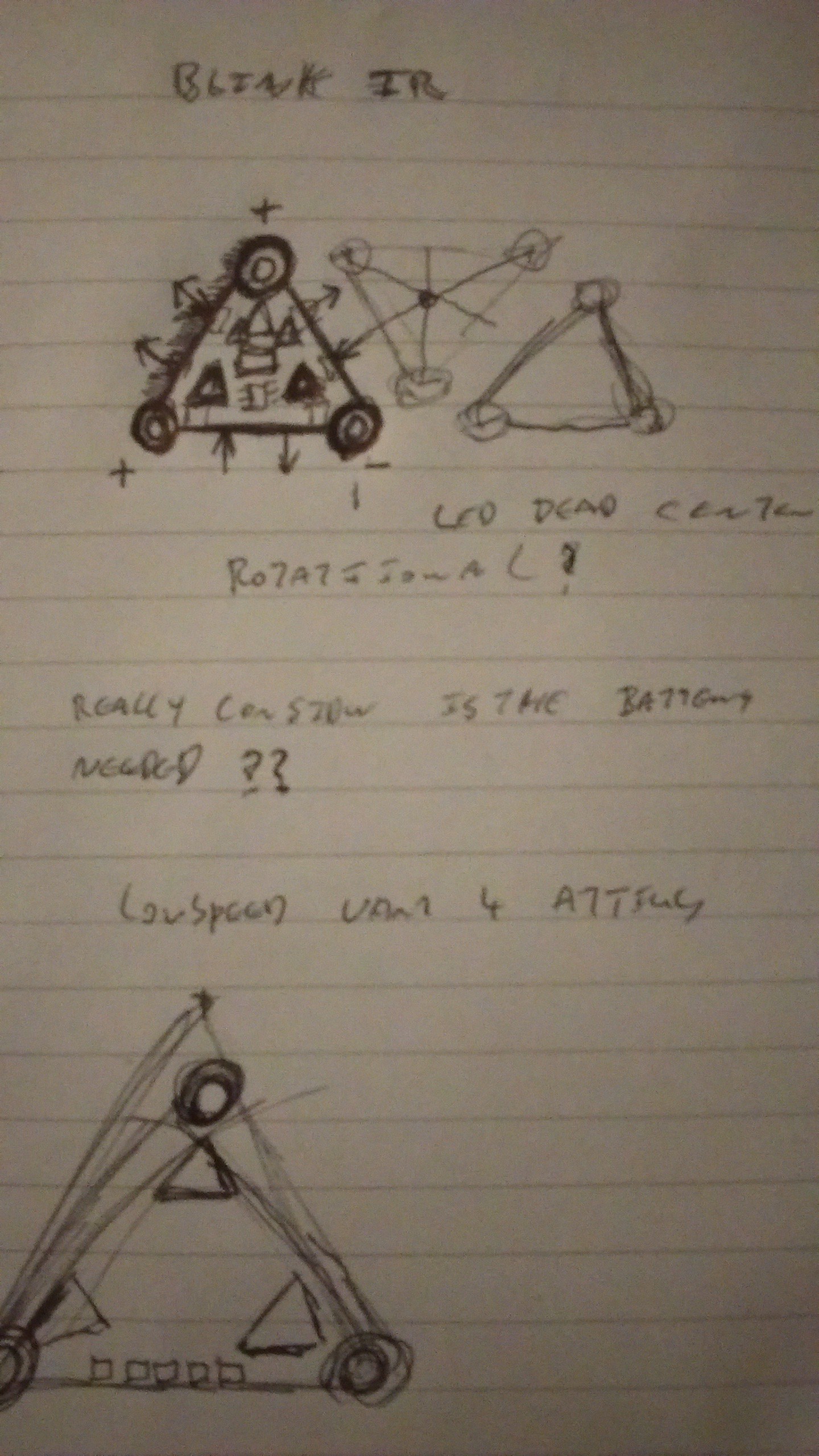
Note in the lower image the 5 small squares at the bottom, these are underside contacts which will be used to program the on-board MCU.
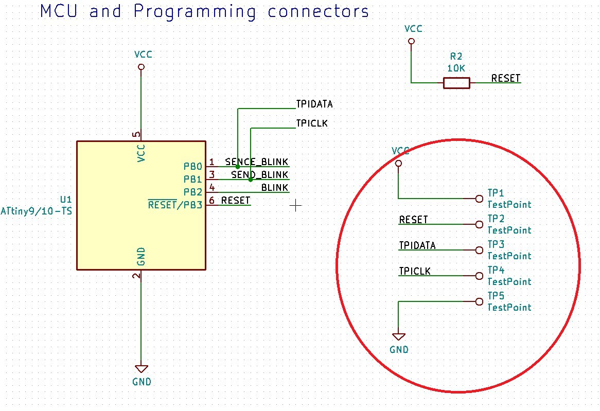
These can be seen on the schematic:
The raced to bring the concept to life:
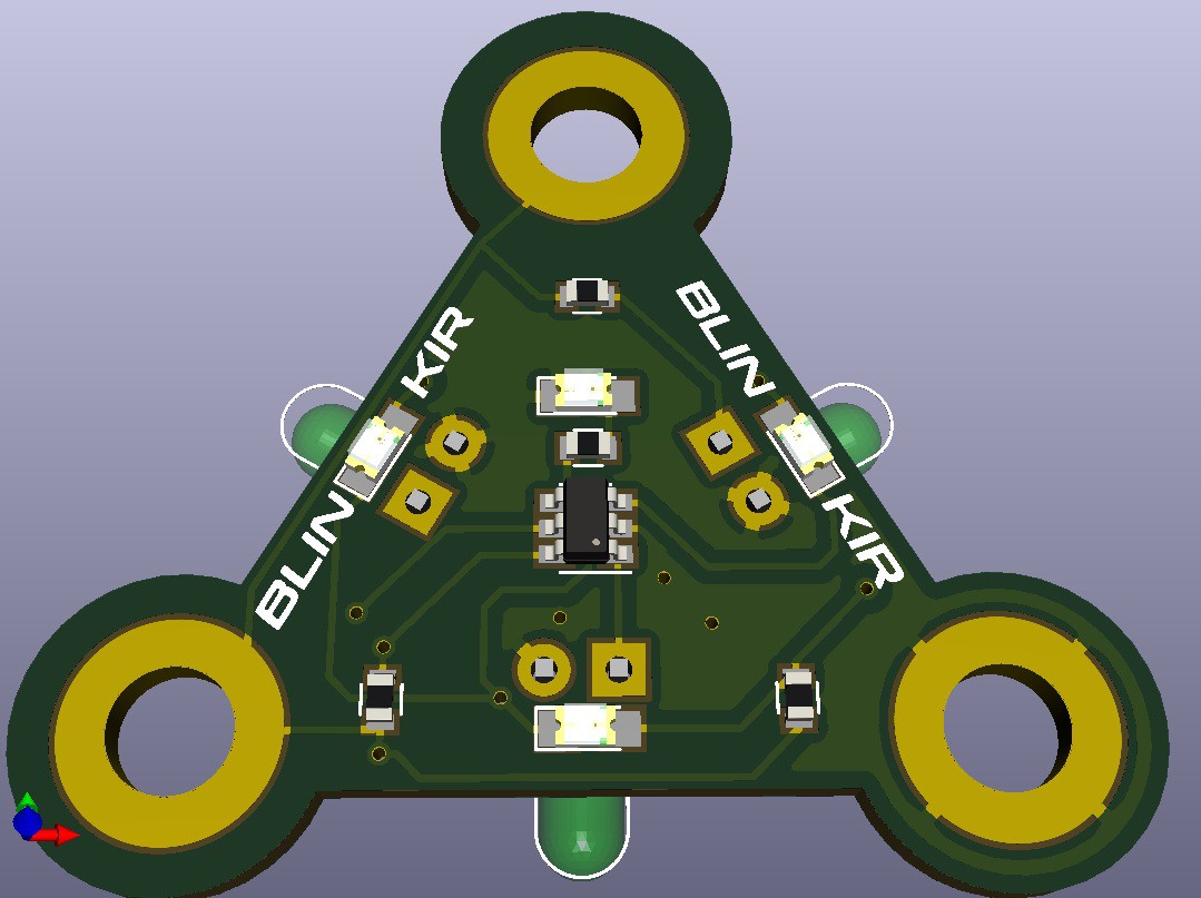
The idea was to try to keep the design and assembly simple as possible the SMT components are on the topside with only 3 through hole placements for the photo transistors. I ended up with this because i wanted to prevent self triggering, avoid double sided SMT placement (with the battery holder it seemed pointless) and i had been testing the IR communications with through hole phototransistors.
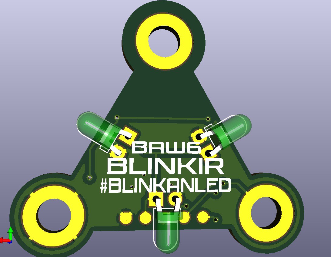
In my own admission the silkscreens where rushed time was running out and needed to get these boards sent for manufacture soon. Also note the programming pads on the underside they are 0.1 inch spaced pads to make a programming jig easy to assemble on some strip/perfboard.
Discussions
Become a Hackaday.io Member
Create an account to leave a comment. Already have an account? Log In.