 greg davill
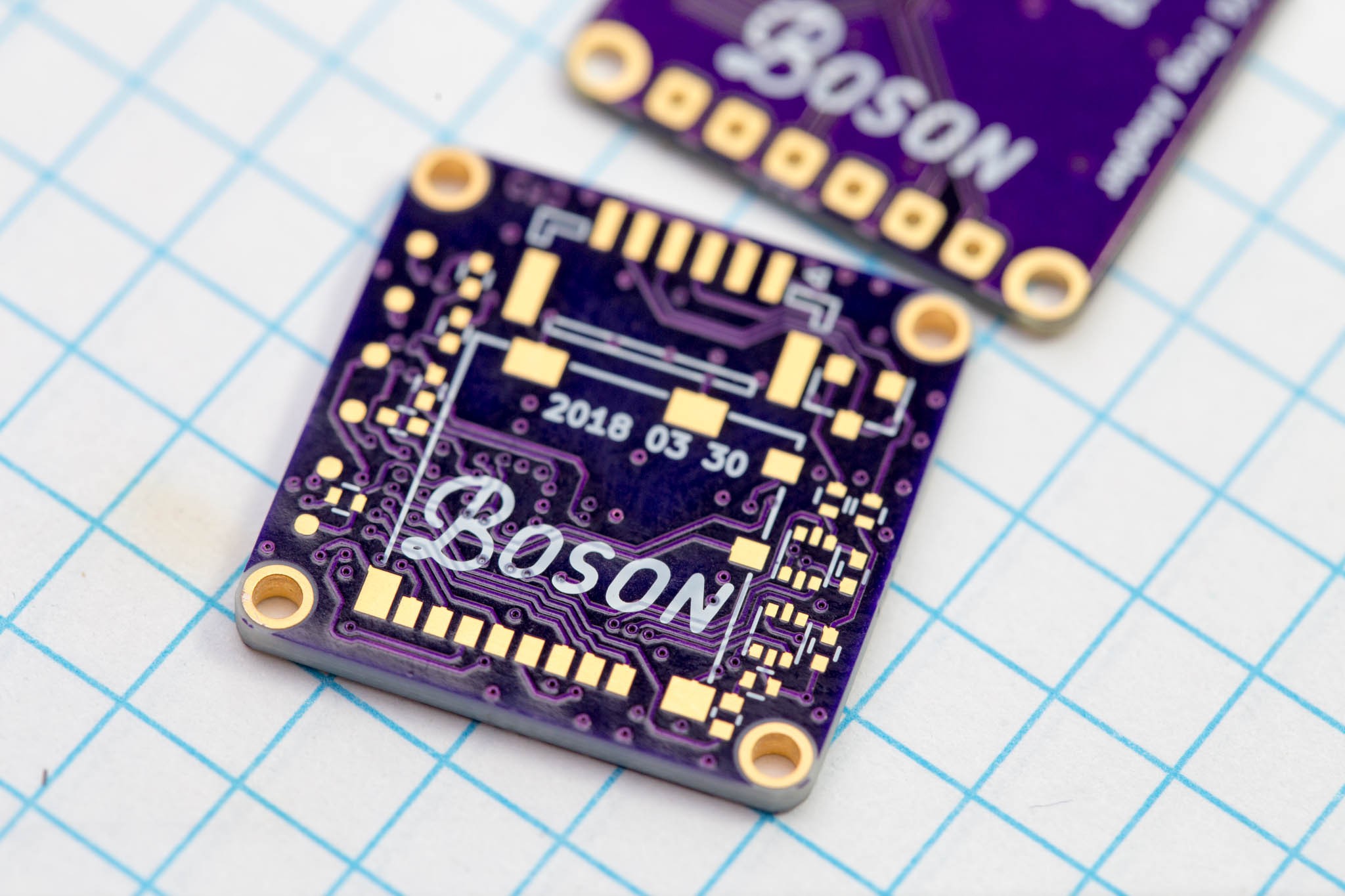
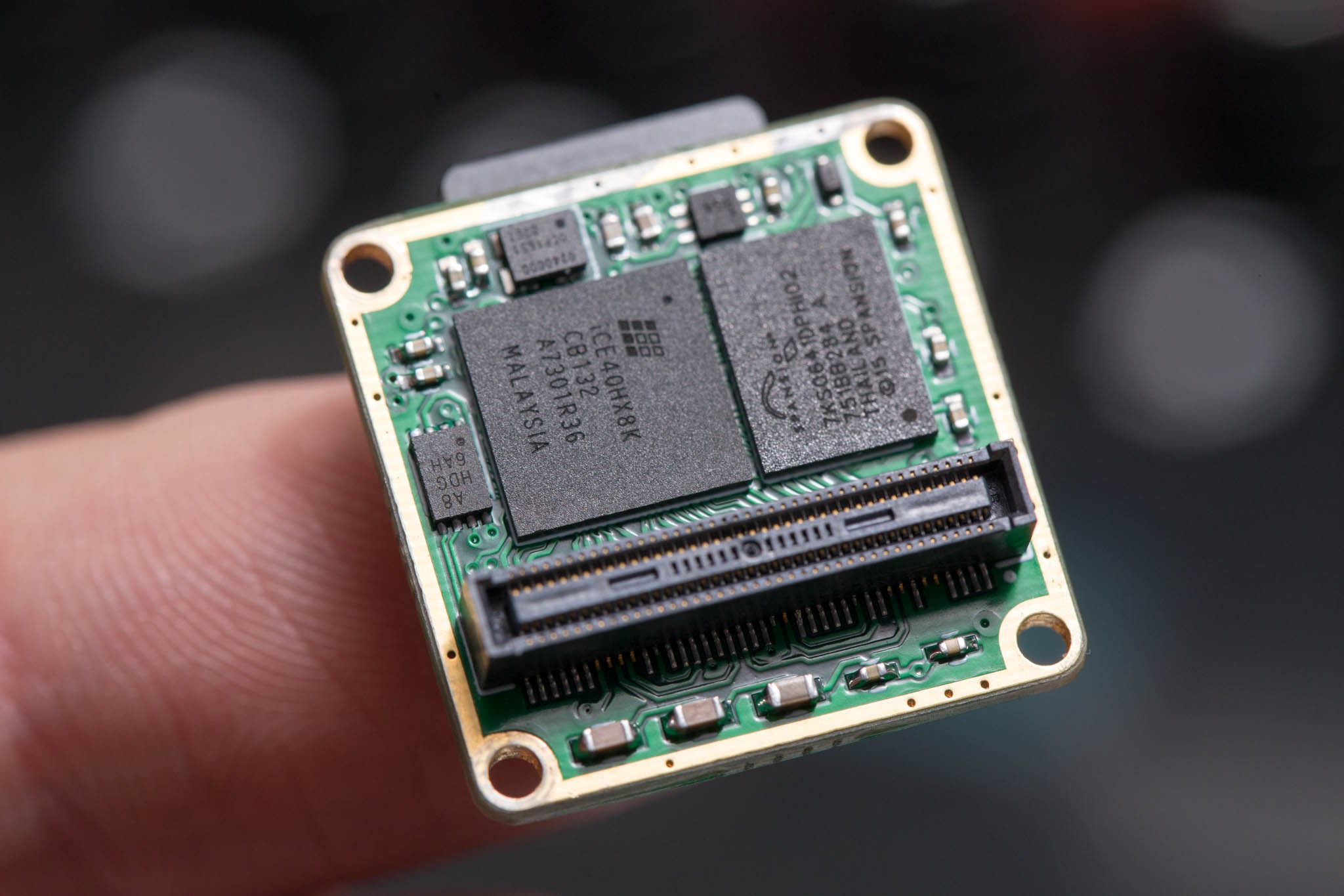
I had mentioned in the last log that I created the footprint wrong for the HyperRAM device. Well my first bosonFrameGrabber PCB had the same errata.
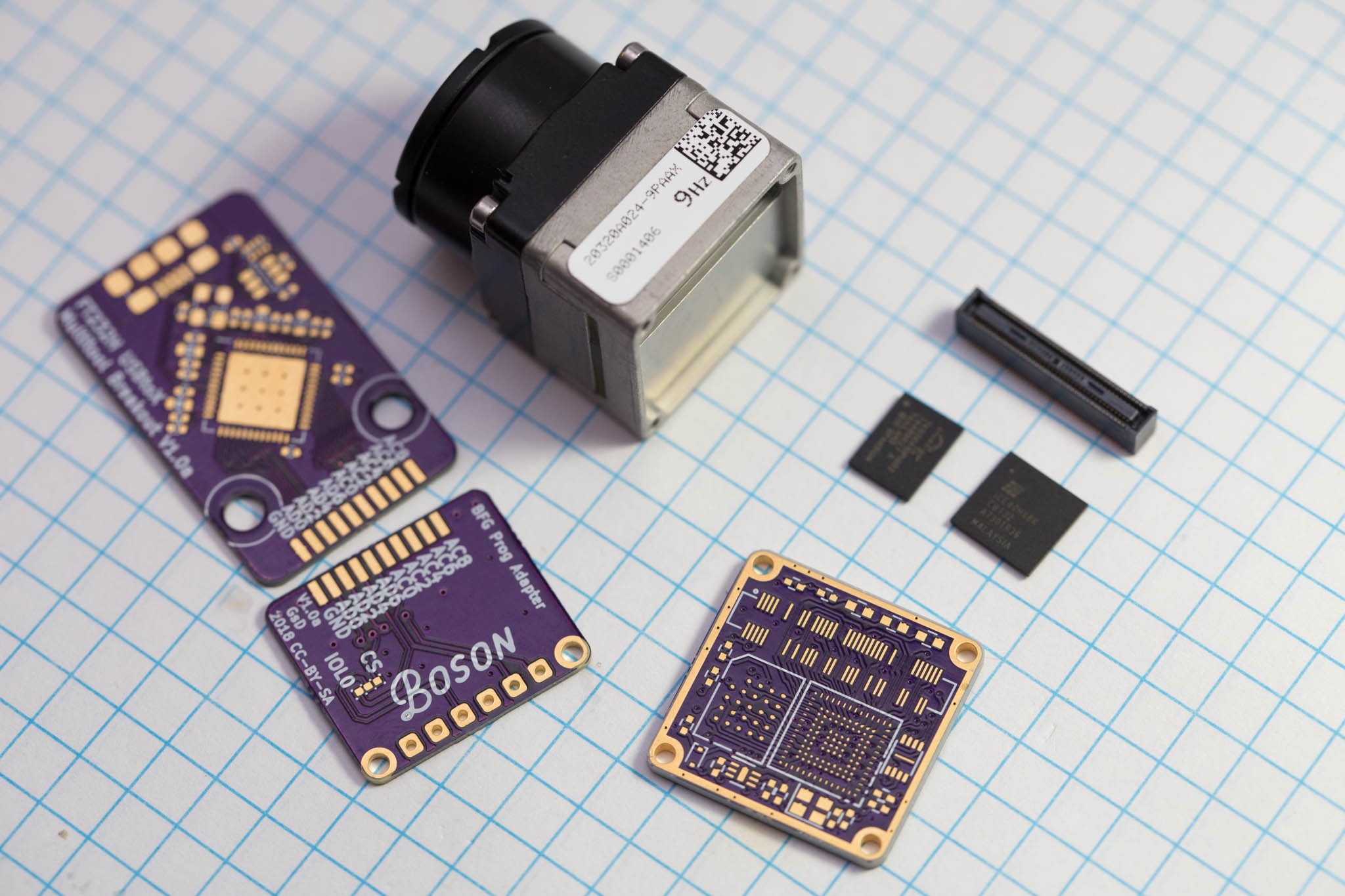
I was able to use this board as a test of my BGA soldering. I'd only ever soldered 0.8mm pitch BGA packages, and the HX8K was in a 0.5mm pitch package! Additionally in order to reduce board size I required a pogo-pin based JTAG connection. Luckily they did not have any errata, and worked great! (My FPGA JTAG programmer is a custom breakout for: https://github.com/esden/ftdi-multitool)
v1_01
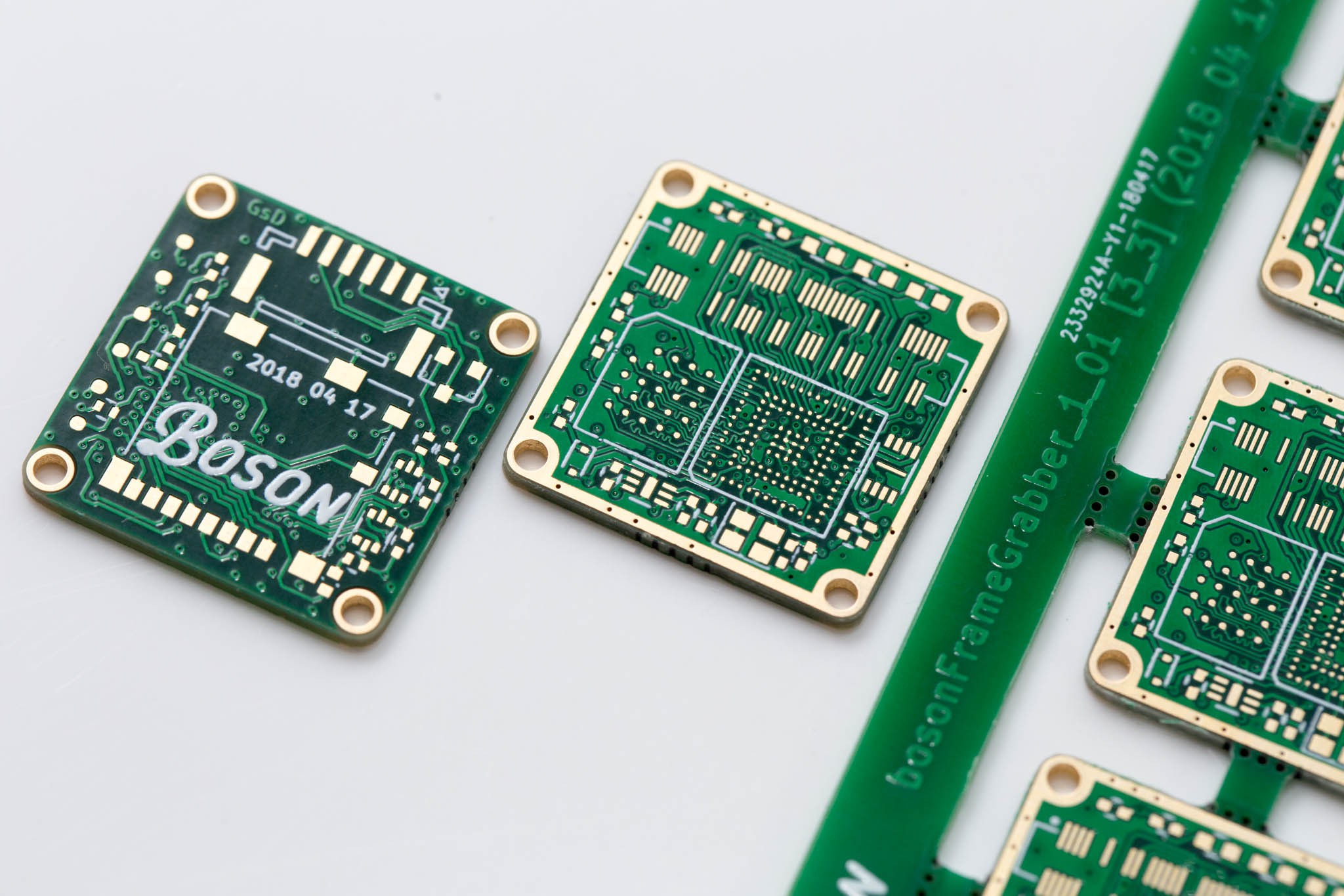
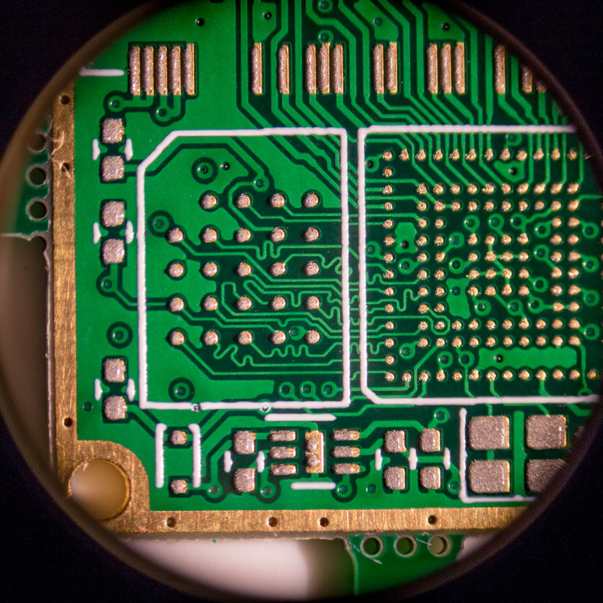
This version had an updated HyperRAM footprint, and was also my first time ordering form JLC PCB. Surprisingly their standard service handles the 3.5/3.5mil trace/space and the 0.2mm drill required for the 0.5mm BGA pitch.
This version actually worked! I was able to port the example project of picosoc over very easily! (https://github.com/cliffordwolf/picorv32/tree/master/picosoc)
Working ontop of a working example is great. Really gives you a nice sandbox to adjust bits and pieces. If anything breaks you can backtrack to your last commit to determine the breaking changes.
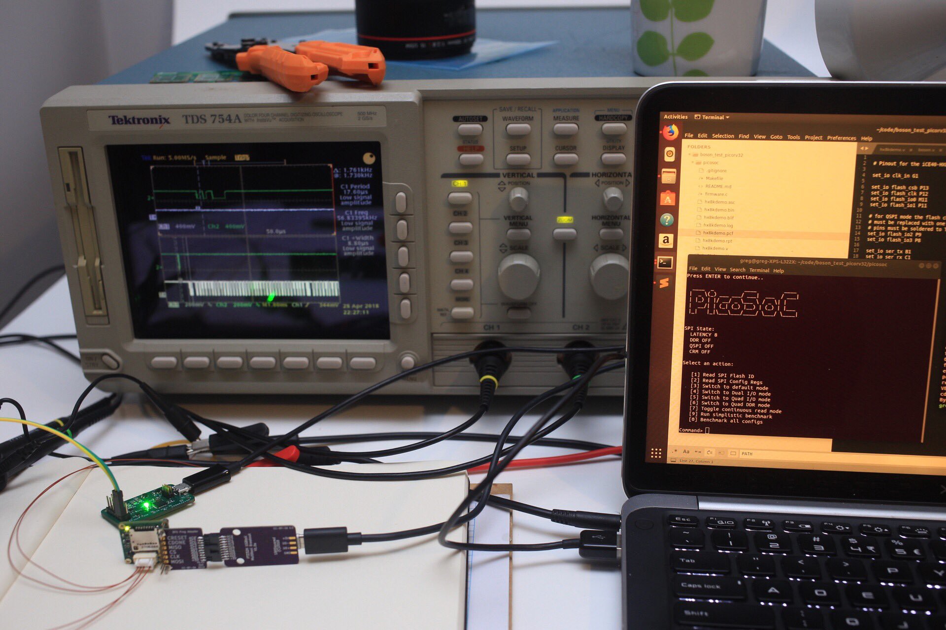
I especially like the basic example code included with picosoc. It's all contained in a single file, and creates a simple prompt that enable you to interact with your hardware though a serial terminal. Adding function stubs to the prompt is super easy. Especially for a firmware engineer like me, it feel safe and familiar.
Over the course of a week I designed up a simple verilog block to capture a parallel stream, GPIO register, hyperram wrapper (based off BML's excelent work https://github.com/blackmesalabs/hyperram)
With these pieces I was able to jump back into firmware, add a FatFs driver using bit-banged IO, and capture this image!
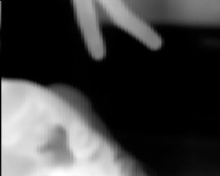
A few issues with this image. I have the endianess wrong in this capture, and I had missed a single DWORD (2 pixels) at the start. But considering how far I had come in a week, this was a success!
Also due to the Bit-Banged SPI SD card interface, this 320x256 pixel image, at 320kb in size (16bbp) took around 15s to save.
Now to optimize!
Discussions
Become a Hackaday.io Member
Create an account to leave a comment. Already have an account? Log In.