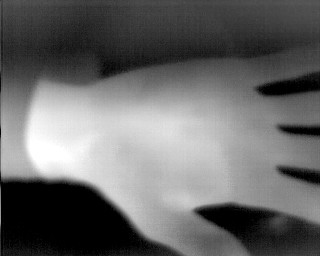
After spending a few weeks tracking down a bug caused by a bad reset circuit and incorrect PLL usage. I've finally captured an image using the new hardware!

It appears that I've lost the first pixel in the frame somewhere into the ether. This results in the single pixel band down the left side of the image.
Still some more work to do in terms of performance. Almost every part of the design can be improved in same way to improve the speed at which I can record these images from the camera module to the SD card.
- SD multiblock write
- SD 4bit mode
- Burst read from HyperRAM -> SD controller
- Use PLL for HyperRAM (4x speed increase)
- Set HyperRAM latency to lowest speed + variable latency (~2x speed increase)
- FatFS f_expand() + single low-level multblock write
The next stage in the project is working on the SD low level drivers to support CMD25 (Multiple block write). When combined with CMD23/ACMD23 (Number of blocks to erase) we can really boost the write speed of the SD card. At this time the image is written in 512 byte blocks to the card, the card accepts this block and performs an erase/write on its internal FLASH. I'm using high quality Samsung cards, and I see this process takes ~1ms

You can see the start of the image being written to the card. The first reads/writes are dealing with the exFAT filesystem, the regular pattern on the right side is the image data written in 512byte blocks, and subsequent busy cycle from the card. The SD card indicates it is busy by holding the DAT line LOW.
You can see that our data cycle and busy cycle are pretty even right now. Data cycle takes ~0.7ms, busy: ~1ms. If we enable 4bit mode now we can decrease the data cycle by 4, but the busy cycle remains unchanged. This results in very little overall speed improvement.
 greg davill
Discussions
Become a Hackaday.io Member
Create an account to leave a comment. Already have an account? Log In.