Top and bottom side of the square inch PCB. Compare the size to an antique 8085 CPU ! The 1.27 mm header is very tiny, never used that before....
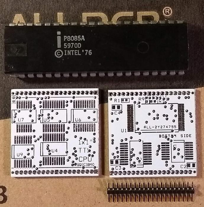
You might have noticed that the last hole on both the headers has no pad around it. Reason is, that with a pad, the pads would come too close to the border of the PCB, according to the design rules of the PCB manufacturer. So I removed the pad there, but the hole is still there, and the headers are placed a little bit out of center so the pad at the other side has enough space. The pins must be connected to a nearby pad with a small wire. For pin 1 (VCC) this connects to C2 (lower left side on bottom), and for pin 40 it connects to a dummy-resistor very close to it (upper right side on top).
Unfortunately, the bigger support pcb's are delayed, and will come after the weekend...
Discussions
Become a Hackaday.io Member
Create an account to leave a comment. Already have an account? Log In.
love it!
Are you sure? yes | no
Yes they look cute !
Are you sure? yes | no