 Benjamin Broce
Early on the PCB layout process, I used an "0603" footprint for most of my passives and my LEDs, and finished what I thought was a great component layout. Everything was fitting a little too well, with lots of extra room... Upon further inspection, I found that the footprints were really 0603 metric, or 0201 imperial, and I was further taught that almost all hobby PCB design and SMD parts are referenced in internet parlance in imperial. There goes my "bigger than a grain of rice" requirement...
After reworking my component sizes up to 0603 imperial, I was finally able to get a good component layout, connected up traces, placed ground planes, and finished my first PCB design!
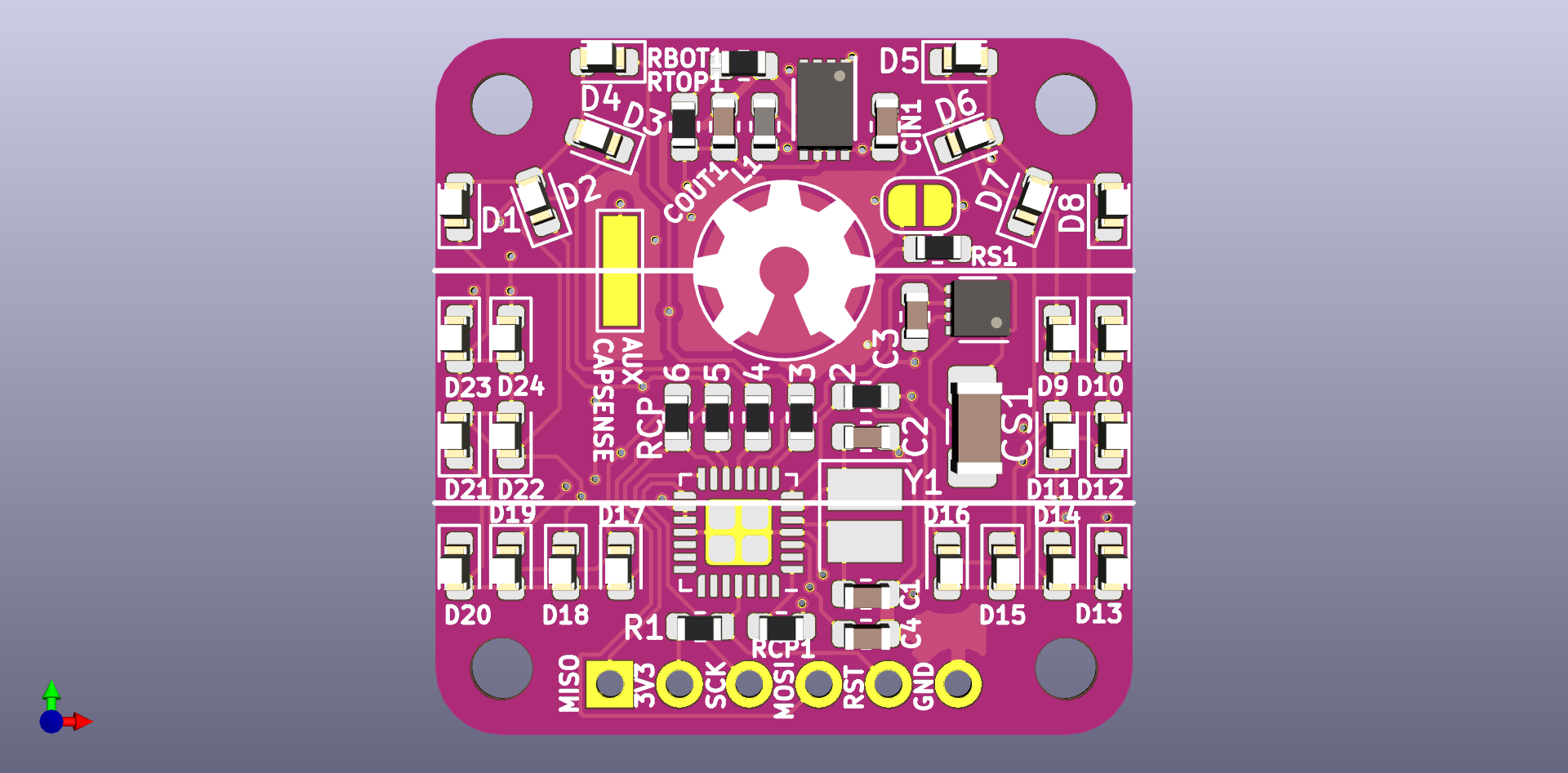
In addition to the LEDs, regulator, ATmega, and cap sense chip, I added a jumper to a pad that could allow an external capacitive touch pad if the 6mm one under the OSHW logo isn't sensitive enough. I also made the footprint for CS1, the capacitive touch sensitivity adjustment cap, 1206, so I could get a few values to experiment with and hand-solder them. Time to whip up a BOM and design an enclosure!
Discussions
Become a Hackaday.io Member
Create an account to leave a comment. Already have an account? Log In.