Universal Supercap Charger
Supercapacitor charging circuit using (mainly) discrete transistors
Supercapacitor charging circuit using (mainly) discrete transistors
To make the experience fit your profile, pick a username and tell us what interests you.
We found and based on your interests.
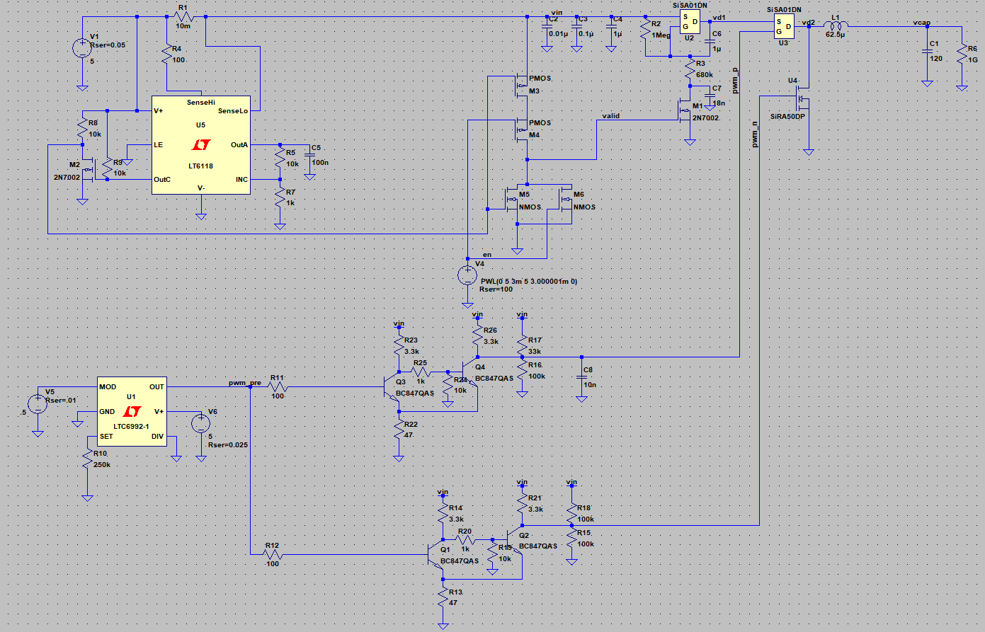
LTSPICE_Schematic_v1.pngLTSPICE Schematic used for first iteration of the chargerPortable Network Graphics (PNG) - 47.51 kB - 10/27/2018 at 14:24 |
|
|

That of course took longer than I would have hoped, but hey no DRC errors and I didn't even fudge the rules this time.
I made sure to add in a ton of vias. Honestly I'm a little worried to check just how many, but hey I have no idea what thermals I need and more can't hurt...
The ground plane has a ton of stitching vias at 2.54mm pitch if I'm not mistaken, though it doesn't really change much. The fact of the matter is that there are a lot of vias connecting the top and bottom ground planes together. Given this thing can take a decent amount of current, I'm not too keen on making anything higher impedance if I can avoid it. It's probably overkill, but so is this project. I could have just bought an IC off the shelf for caps, but no. I want my programmable current limit (resistor based as of now) and awkwardly placed test point silk-screen labels damn it.
That being said, those vias better be tented or so help me. No literally, I'm going to need a lot of help getting those parts to where they need to be as I won't be able to read the damn legend.
As a warning to those with trypophobia, you don't want to read on. This is your last chance!
Read more »
With the layout now complete, now routing and then off to the board house it goes. Of course if DRC doesn't give me a headache.
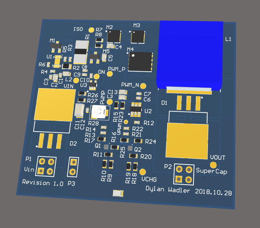
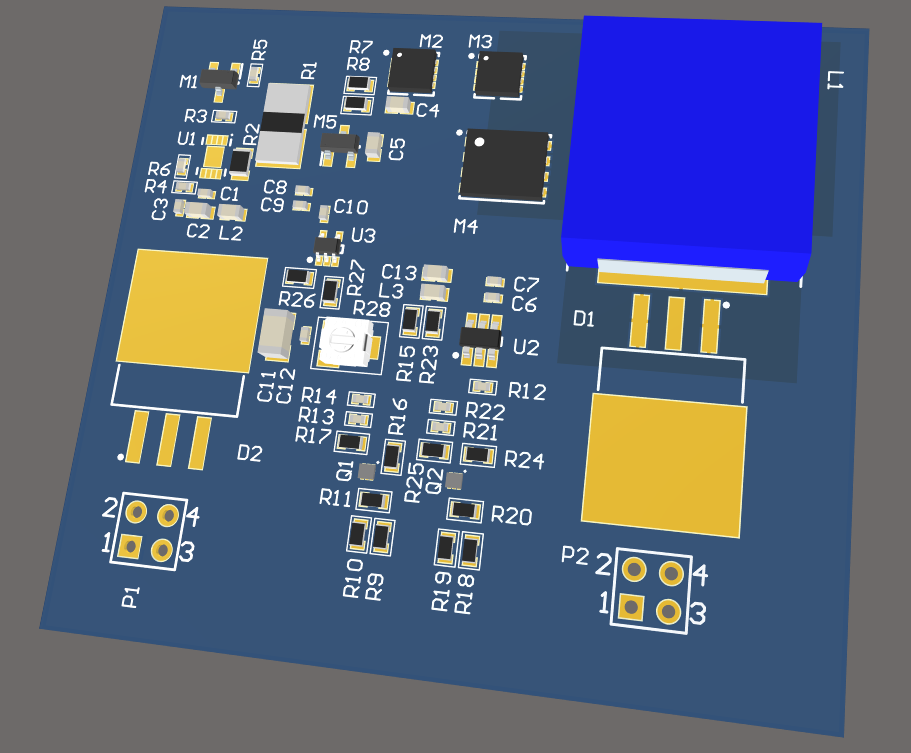
While being compact is certainly an end goal, testing will be a hell of a lot easier with a single sided board. Soon enough the 2 x 3.25 in board will be able to be shrunk. Probably put all the timing controls on the bottom, leave the big stuff on top for ease of manufacturing.
This board isn't anything fancy, just 2 layers, normal tolerances etc. Those dinky little double BJT packages (Q1, Q1) though are laughable given the comparison to that massive inductor in the top right corner (L1). Of course after looking at it, now I see that L1 is facing the wrong way. No big deal, but kind of annoying given everything else is fine.
The two connectors towards the bottom corners are the input and output connections. One for power in, the other for connecting to the supercapacitor. I thought it would be better to make it more universal without soldering the cap to the board, though for later revisions having presoldered caps would be nice.
All that's left to add in is some test points and maybe two or three mounting holes, because why not? Also can't help but add in some fun silkscreen stuff later on, but that'll be for later today.
Now on to routing!

After roughly a total of 30 hours of SPICE simulation, I have managed to create a decent design for charging a 120F supercapacitor at 5A to roughly 2.5V in under a minute. There were a number of problems such as inrush current, various spikes of more than 200A at initial start, and sometimes a runaway current increase. These problems have been solved with an enable input, a modified synchronous buck converter design, and a current sense feedback.
I wasn't too happy about requiring the current sense amplifier, but I don't think there is another way to limit the current without increasing the power dissipation of the MOSFETs. I did find that the 18nF capacitor (C7 in the LTSPICE schematic) with the 680K resistor created the time constant to allow for the charging current to be limited without fully turning off the system and thus causing the supercapacitor to start to discharge.
I'm thinking of using a 74AUC1G02 instead of the discrete NOR gate implementation for simplicity reasons while testing, as again the SPICE simulation failed to converge otherwise.
One addition that I did not include in the LTSPICE schematic, is a SM74611 diode for reverse polarity protection when the charging circuit is disabled. As I'm still trying to figure out how exactly to connect the circuit as a charger with a connector (as in what point of the circuit to break), I think the most reasonable point is after L1 (again in the LTSPICE schematic) and using that low forward voltage diode (25mV at 8A!!!) seems to make a lot of sense. Given that I don't want to add in a ton more transistors to force U3 and U4 to be off when disabled, putting a diode after L1 makes more sense. I did run simulations with a generic diode for testing purposes, and there wasn't a problem with it, save for the forward voltage causing problems of course. The SM74611 would cause the simulation to run a ton slower which obviously isn't ideal.
For future additions, having a way to stop the rest of the circuit from being used while charging may be useful. Adding in another PMOS transistor with the gate tied to the inverted output of the NOR gate driving M1 would provide a simple solution. But having a device shut off when the charger is plugged in isn't exactly ideal.
Another addition is using an auto-enable for the charge circuit. Given enabling the circuit immediately after a voltage is present isn't ideal, mainly due to the fact that the LTC6992 needs about 2ms to start the PWM cycle, using a RC filter with an inverting schmitt trigger would provide this functionality due to the active low enable input ( simulated by V4). Not including this right now would allow for more flexibility in the design, such as using a microcontroller to drive the signal if desired.
I have also been toying with the idea of increasing the input voltage from 5V to 10V just to further reduce the dutycycle of the buck converter, but that would put more strain on the NMOS I would think. It does have 100W dissipation limit as opposed to the PMOS at approx 33-52W (depending on junction temp) so offloading it may be useful without reducing the charging rate. More testing has to be done. However, when trying to simulate this I ran into problems with the drive circuitry for those transistors as they were stuck at voltages which causes a massive current avalanche. Though with the current sense now, this may be ok. More work has to be done of course, and this will definitely increase the efficiency.
Create an account to leave a comment. Already have an account? Log In.
Become a member to follow this project and never miss any updates