 Tony
Tony
Probing other ways to generate high voltage
Seeing the first prototype work, it got me thinking. Do I really need to use this expensive LT3757 switching regulator? Is a flyback really better than a traditional boost converter if I use good parts for it? Should I test my theory that the dual diode is absolutely useless and a drag on performances?
Before taking this project further, I had to answer these questions.
So I decided to go ahead and launch a new set of prototypes, based on Texas Instruments’ LM3488. According to TI, the LM3488 is a “versatile low-side N-FET high-performance controller for switching regulators. This device is suitable for use in topologies requiring low-side FET, such as boost, flyback, or SEPIC.”; with a maximum output voltage of 500V.
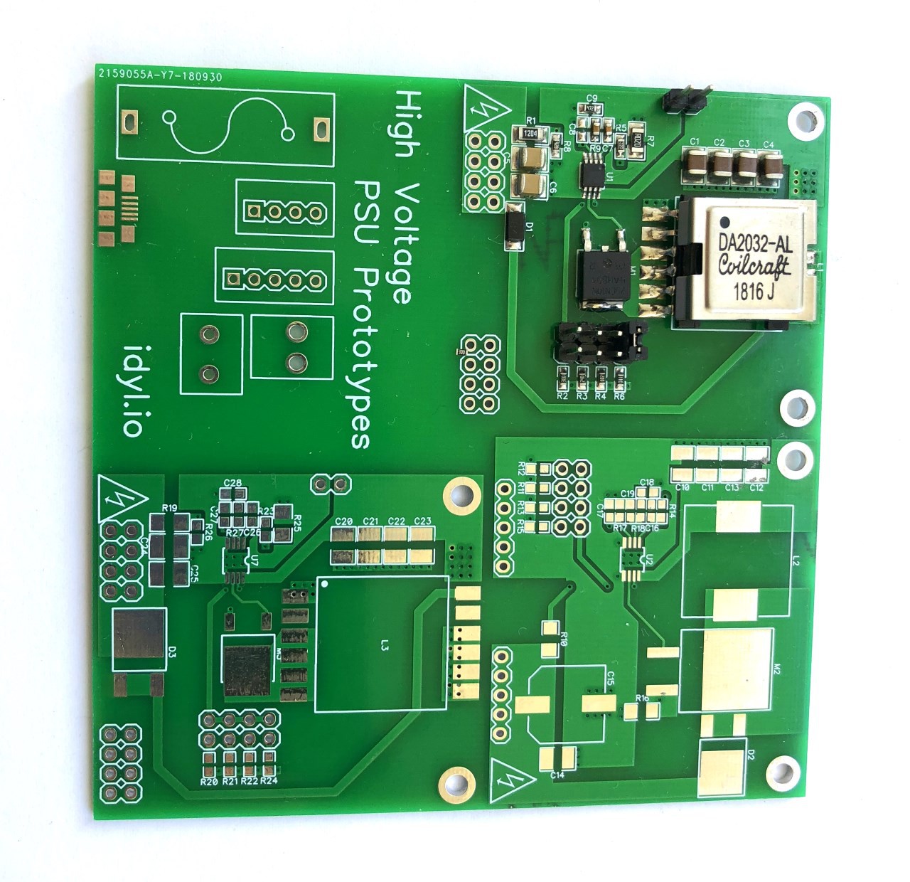
It’s also a lot cheaper, and has simplified input/outputs with only 8 pins versus 11 for the LT3757. I thought to myself that maybe, just maybe, I was overengineering this power supply.
For this prototype I also included some jumpers that allows me to select different switching frequencies to see the effect it would have on efficiency.
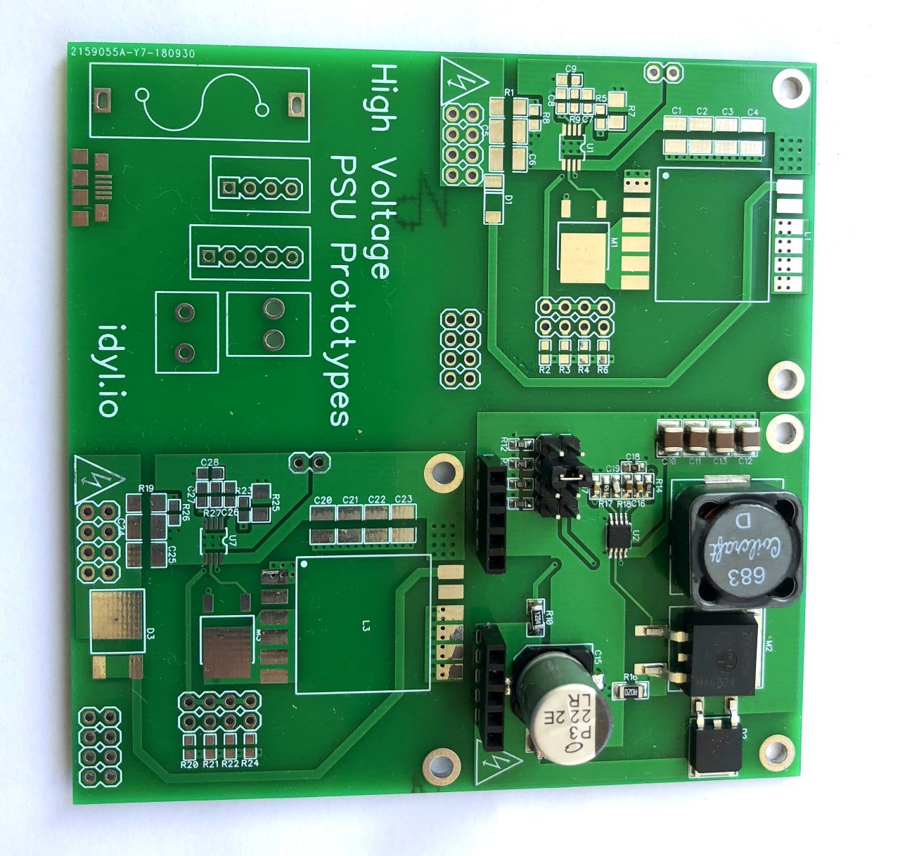
The last prototype on the board is the same version as the first one, except it uses another transformer, the DA2033. It’s a bigger version of its little brother. Since I had space left on the PCB, I just wanted to experiment with this other transformer.
None of these designs gave me good results. To this date I don’t know why. Did I do something wrong? Are TI chips a bit more stringent on what they can accept? I do not know. However, it comforted me in my idea that the LT3757 was pretty darn nice in comparison.
Revision B of the prototype
After this brief interlude I worked on the revision B of the power supply.
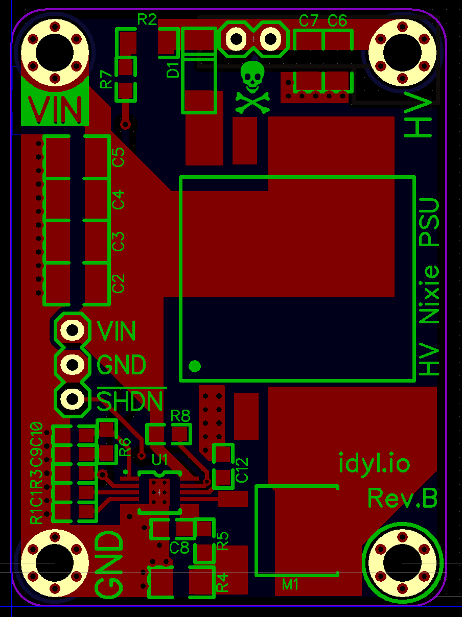
A few improvements on this version:
- The Shutdown pin is now accessible.
- No more snubber network.
- Direct connection between input voltage and the primary (no more vias).
- The switching diode has been updated to a RFN1LAM6STR.
- High Voltage side moved completely at the top of the board, replacing a long trace going back to the bottom.
- Better silkscreen
When looking for a change of diode, I needed something FAST; with very little leakage. With a recovery time of 35ns and 1uA leakage @ 600V, this diode is a killer so I thought I’d give it a try.
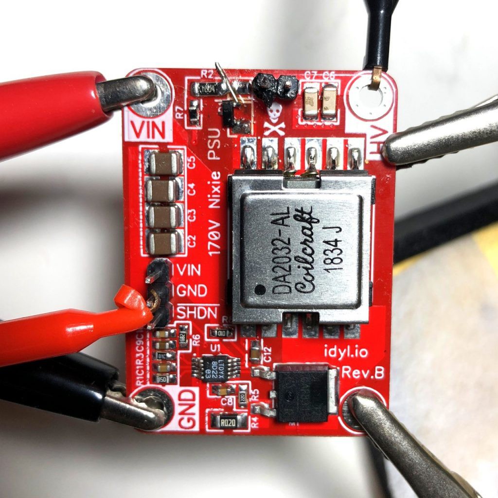
On the picture above, don’t pay attention to the botched up job on the diode at the top, it was just an experiment I was running to see what was the impact of the dual diode versus the newly selected fast recovery diode. The answer to this question is: actually not so much difference. I still don’t understand why Linear’s engineers chose this more than average part in their reference design. There are so many good diodes out there, why this one? I doubt I’ll get an answer to this question.
Discussions
Become a Hackaday.io Member
Create an account to leave a comment. Already have an account? Log In.