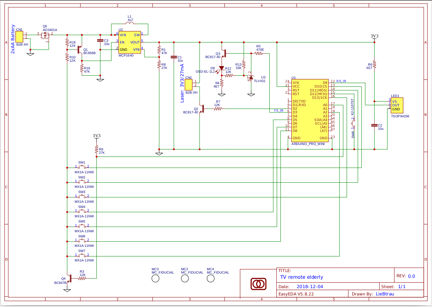
First draft version

Issues:
- No switch for reprogramming
No LED to show user that programming succeeded.The laser diode can be used to that purpose.- Risk of latchup through switches. They immediately pull up the GPIO, while the boost converter has yet to start.
- SPI lines should remain free for maybe future addons.
First prototype

Issues:
- R18 must be increased, because the unpowered GPIOs have a too high impedance. 33K as a replacement for R18 seems to work fine.
- R9 is needed to enable Q4 on startup. The problem is that it prevents the circuitry from powering down.
Measurements
- Total current consumption in power down mode (EN=low) : 700nA
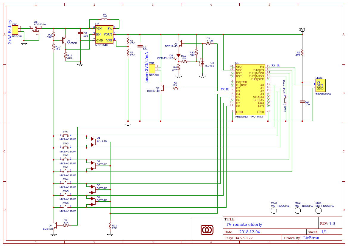
Revision 1 : as patched on R0 PCB

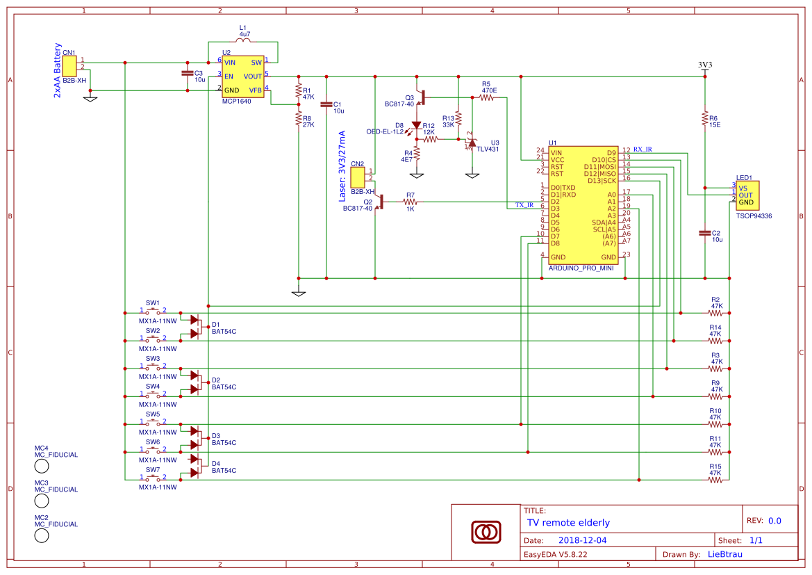
The previous designs had problems with reliable startup. Either the unit didn't boot or it couldn't be turned off. This R1.0 design fixes those issues.
To startup, R10 must be pulled down. This happens when a user presses one of the switches. The schottky diodes conduct and R10 gets pulled down through R11.
Once booted, the firmware will pull up R3. Q4 starts to conduct and the button could be released.
The firmware still needs to read what button has been pressed. On the side of the MCU, internal pullups will be used. The low impedance path from the switches to GND (through R11) must be disabled. So D4 will be pulled up. From then on, the MCU can read the state of each switch.
Once the switches are released, the device will be turned off by pulling R3 low. The device will not immediately turn on again, because there's no low impedance path from R10 to GND. R3 has no pullup to 3V3, so there's no way it would be pulled up after the MCU switched off.
 Christoph Tack
Discussions
Become a Hackaday.io Member
Create an account to leave a comment. Already have an account? Log In.