- Part 1: How the sound is made
- Part 2: How the CPU does what
- Part 3: Writing the first ROM file
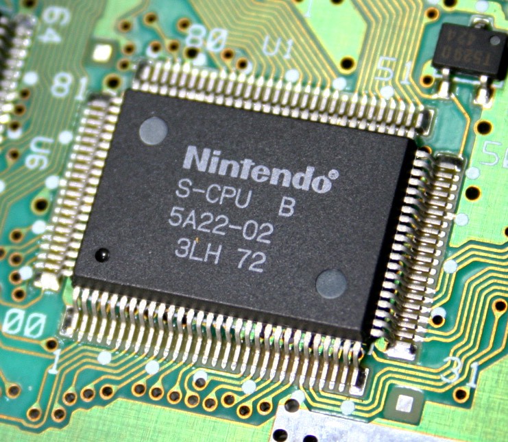
Let's start from the top here and work our way down... The CPU in the SNES is the Ricoh 5A22.

The 5A22 is a Microprocessor, so it has a CPU and peripherals. In addition to the 65C816 CPU core, the 5A22 includes:
- Controller port interface circuits, including serial access to controller data
- An 8-bit parallel I/O port, which is mostly unused in the SNES
- Circuitry for generating non-maskable interrupts on V-blank
- Circuitry for generating interrupts on calculated screen positions
- A DMA unit, supporting two primary modes:
- General DMA, for block transfers at a rate of 2.68 MB/s
- H-blank DMA, for transferring small data sets at the end of each scanline outside of the active display period
- Multiplication and division registers
- Two separate address busses driving the 8-bit data bus: a 24-bit "Bus A" for general access, and an 8-bit "Bus B" mainly for APU and PPU registers

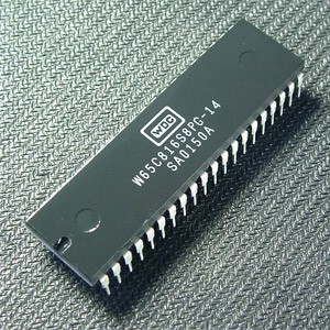
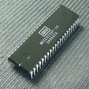
The 65816 core is an enhanced version of the 6502, which is an 8-bit core. So, 65 in the name means it's compatible to the 6502, and 816 means the possibility to switch between 8- and 16-bit register sizes.

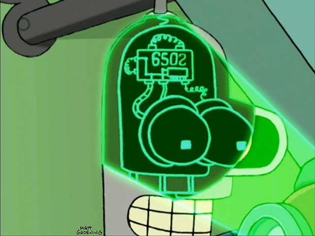
So, in the beginning there was the 6502. It's used in personal computers and consoles such as the Apple IIe, the Commodore PET, the Atari 2600, the Commodore 64, the original NES and Bender from Futurama.

Then, there was the 65816, which was an enhancement with higher clock rates and bigger register sizes. It's used in the Apple IIG and the SNES.
The 65816 is (almost completely) backwards compatible with the 6502 and even has an emulation mode that is automatically initialized when the processor is powered up.
So, to understand the 65816, we need to understand the 6502, and luckily, many many people have spent lots of time doing so. There's even this visually animated emulator for the 6502: http://www.visual6502.org/ It only exists because Michael Steil took the lid off of the 6502 and actually made microscopic photographs of this legendary device. He did a talk on this work and you can watch it here: (bottom)
When I learned that the SNES CPU is actually an enhanced 6502, it was even more reason for me to do this project because I often fantasized abpout programming a 6502 in real life. :) Programming doesn't get anymore "bare-bone" than 6502. ;) So, the 65816 takes opcodes which you can find in tables, but most people used to program this chip in assembler which is then "assembled" to opcodes that are directly readable by the processor. These machine codes are stored in external memory, because the 5A22 has no built in memory. This external memory is actually just the cardtridge! When the 5A22 is powered up, it loads the first adress on its 24-bit adressbus, this bus is hardwired to the ROM, which reacts and presents the first opcode for the processor. After processing the first command, the processor now wants another operand or increments the program counter to read the next command, which again is presented on the adress bus and the ROM reacts and puts data on the 8-bit databus. So, this is exactly the bahaviour that we will have to simulate for the processor! Doesn't sound too complicated, right? Read an address, look up the data on this address and present the data! Well... turns out it's actually really that easy! :D Yeah well almost, as you will see.
Someone has actually already done something similar with an ARM processor. You can find this project here: https://dhole.github.io/post/gameboy_cartridge_emu_1/ It's really interesting and you can already see some problems that we will encounter much later in this project.
If you want to read more about the 65816, such as the opcodes or other technical details, I can recomend this page on the superfamicom wiki: https://wiki.superfamicom.org/65816-reference
They also link to datasheets by Western Design Center (WDC) for the 65816, which is really cool, because one thing that's really sad, is that there are no datasheets for the 5A22. :/ This is also where the reverse engineering work will happen and I can promise you some really cool stuff coming up, such as a complete logic analyzer capture of SNES-to-ROM-communication! <3
Alright well, next part will be writing a ROM file and the first machine codes for the SNES. This is going to be really exciting, especially because I'll show you how to setup your own development environment for the SNES.
Cheers,
Mike
 Foxchild
Discussions
Become a Hackaday.io Member
Create an account to leave a comment. Already have an account? Log In.