 spudfishScott
Each Spikeputor instruction is one word (16 bits) long, with a subset of the instructions requiring a second 16-bit integer. Operations are divided into four groups: ALU Functions, Branching, Load, and Store.
ALU Functions
All ALU operations require two source operands, and one destination register. The two source operands are either two registers (Ra and Rb), or a register (Ra) and a 16-bit signed integer literal. The result of the ALU function is then stored in the destination register (Rc). Thus, ALU functions may either be one word or two words long, depending on the need for the 16-bit constant. Two-word instructions end in C.
ALU Instructions:
- Arithmetic
- ADD(Ra, Rb, Rc)
- SUB(Ra, Rb, Rc)
- ADDC(Ra, const, Rc)
- SUBC(Ra, const, Rc)
- Bitwise Logic
- AND(Ra, Rb, Rc)
- OR(Ra, Rb, Rc)
- XOR(Ra, Rb, Rc)
- ANDC(Ra, const, Rc)
- ORC(Ra, const, Rc)
- XORC(Ra, const, Rc)
- Bitwise Shift: The bottom four bits of the second operand represents the number of bits to shift. SRA is a right shift with sign extension.
- SHL(Ra, Rb, Rc)
- SHR(Ra, Rb, Rc)
- SRA(Ra, Rb, Rc)
- SHLC(Ra, const, Rc)
- SHRC(Ra, const, Rc)
- SRAC(Ra, const, Rc)
- Compare: Rc is set to 1 if the comparison is true, 0 if not. Comparisons are based on 2's complement signed integers except for CMPUL, which is an unsigned compare less than.
- CMPEQ(Ra, Rb, Rc)
- CMPLT(Ra, Rb, Rc)
- CMPLE(Ra, Rb, Rc)
- CMPUL(Ra, Rb, Rc)
- CMPEQC(Ra, constant, Rc)
- CMPLTC(Ra, constant, Rc)
- CMPLEC(Ra, constant, Rc)
- CMPULC(Ra, constant, Rc)
Branching
Conditional branch instructions test the value of register Ra. The branch is taken if Ra is zero (for BEQ) or not zero (for BNE). The second word of the instruction is used to specify a 16-bit signed Program Counter offset. Before the branch, register Rc is loaded with the next calculated Program Counter value so it may be used as a return vector. If the branch will be followed, the target branch address is calculated by adding the given offset to that new PC value.
For immediate branching, there are two options: JMPC calculates the target branch address by adding the value of Ra to the given 16-bit signed literal. JMP simply takes the target branch address from the value of register Ra. As with the conditional branches, Rc is set to the address of the subsequent instruction. Branch instructions are two words long except for JMP. Also, if Ra is register 6, the JMP(R6, Rc) instruction will clear the IRQ flag, indicating the end of interrupt processing.
Branching Instructions:
- BEQ(Ra, PC offset, Rc)
- BNE(Ra, PC offset, Rc)
- JMPC(Ra, mem offset, Rc)
- JMP(Ra, Rc)
Load
There are two load instructions to move values from memory into registers. Both instructions use two words, the second of which is used as a signed memory offset. For the LD instruction, the target memory address is calculated by adding the value of register Ra to the given offset . The LDR (LoaD Relative) instruction adds the offset to the memory address of the subsequent instruction. In both cases, the data in the calculated memory address is stored in register Rc.
Load Instructions:
- LD(Ra, mem offset, Rc)
- LDR(PC offset, Rc)
Store
The only way to write to main memory is through the two-word Store instruction. The value of register Rc is stored in the memory address calculated by adding the value of register Ra to the value of the second word.
Store Instruction: ST(Rc, Ra, mem offset)
The format of the opcodes are as follows:
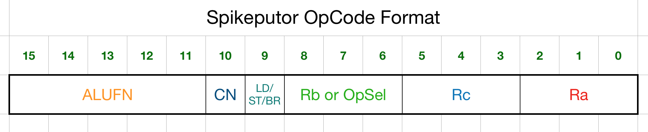
The top five bits of the opcode are simply the ALU function (described in the ALU log entry) and are passed directly to the ALU. Bit 10 (Constant Needed) indicates whether or not the opcode is made up of a one word or two words. Bit 9 differentiates between ALU functions and the other Spikeputor operations (Load/Store/Branch). If bit 9 is clear, the next three bits (bits 8-6) encode the register address of the second operand, Rb. The Rb bits are ignored for ALU functions that use the second word as a constant. If bit 9 is set, the instruction is determined from bits 8-6 as follows:
- 0b000: JMP
- 0b001: <undefined>
- 0b010: LD
- 0b011: ST
- 0b100: BEQ
- 0b101: BNE
- 0b110: LDR
- 0b111: <undefined>
Bits 5-3 encode the register address of Rc, and bits 2-0 encode the register address of Ra.
Control Logic
The control logic of the Spikeputor translates the opcodes plus a few flags into a series of control signals. The signals select the appropriate CPU phase, keep track of the IRQ status, and set up the appropriate logic paths in order to execute the current instruction. Signals, flags and control logic are described in detail below.
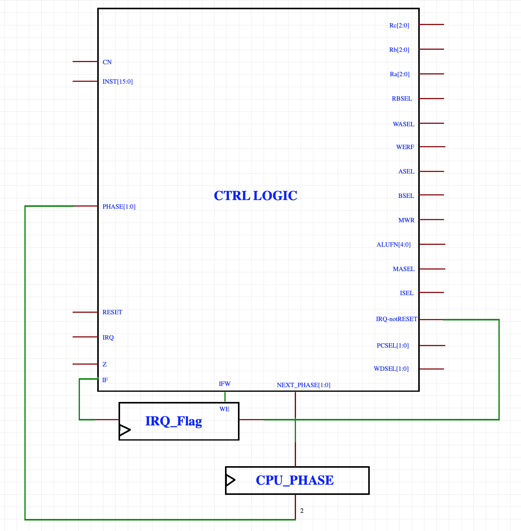
Each instruction takes two or three clock cycles (CPU phases) to perform. The PHASE signal keeps track of these steps. Upon reset and power-up, PHASE is set to 0.
Control Logic Inputs are as follows:
- The input CN (Constant Needed) is directly wired to bit 10 of the main memory data output.
- INST is the 16-bit output of the INSTRUCTION Register.
- RESET is the hardware reset line.
- IRQ is the hardware interrupt line.
- Z is the output of Zero Detect logic applied to the Register Memory Channel A output.
- IF is the output of the IRQ_Flag status bit.
When PHASE is 0 and there is no RESET or IRQ signal, an opcode is read from the memory address pointed to by the Program Counter (PC) register and placed on the input of the INSTRUCTION register, to be stored on the next clock pulse. CN is immediately used to determine if a second word needs to be read for the instruction.
If CN is 0, NEXT_PHASE is set directly to 2 and the PC will not be incremented. Otherwise, NEXT_PHASE is set to 1 and the PC is incremented. On the next clock cycle, PHASE will be 1. Memory at the new PC address is read into the CONSTANT register and the INSTRUCTION register is not updated (It will still contain the instruction opcode from Phase 0). NEXT_PHASE is set to 2 and the PC is not incremented.
On the next clock cycle, PHASE will be 2. This is the phase where the instruction is executed. The ALU function, register addresses, and all other logic pathways will be set based on the Control Logic Inputs. The PC will be updated (either incremented or updated with the new "jump to" address), and NEXT_PHASE is set back to 0, starting the next instruction cycle.
If the RESET signal goes high at any time, PHASE is reset to zero, the IRQ flag is cleared, all memory write and register write signals are cleared, and the NEXT_PC register is set to the Reset vector via the PCSEL signal (described below).
If the IRQ signal goes high, RESET is low, the IRQ_FLAG (IF) status bit is currently clear, and PHASE is zero, the IFW (the IRQ Flag Write) signal is set so that on the next clock pulse, the IRQ_FLAG will be set. R6 is set to be written to with the current PC address, and NEXT_PC is set to the Interrupt vector via the PCSEL signal. The IRQ signal is ignored if IF is already set, PHASE is not zero, or RESET is high. Systems invoking the Spikeputor IRQ signal should only set it during CPU phase 0. The BIAS card will capture this information by looking at the ISEL signal, which is high only during that phase.
The remaining signals have the following meanings and are mainly used to set up the logic pathways for each instruction. Each signal is one bit unless otherwise noted. See the Spikeputor Main Schematic for the high level view:
- Ra, Rb, Rc (3 bits each) are the three register address inputs to the Register Memory module. They are directly copied from the appropriate bit fields of the opcode as described above. Ra specifies which register address is output on Register Channel A. Rb and Rc are used as described below.
- RBSEL selects whether the Rb or Rc operand from the opcode specifies the register address to output on Register Channel B (0: use Rb, 1: use Rc).
- If WERF is high, the WData Input is written to the selected input register on the next clock cycle. If WERF is low, the previous value of that register will be maintained. The input register is determined by Rc and the value of WASEL.
- WASEL selects whether the input register is set to Rc or if the exception register (R6) will be written to (0: use Rc, 1: use R6).
- ALUFN (5 bits) is sent directly to the ALU to select ALU function and output channel. These five bits are directly copied from the opcode as described above.
- ASEL selects whether ALU Input Channel A will come from Register Memory Output Channel A or from INC_PC, the incremented value of the program counter. (0: Register Memory, 1: Program Counter).
- BSEL selects whether ALU Input Channel B will come from Register Memory Output Channel B or from the CONSTANT register (0: Register Memory, 1: CONSTANT).
- MWR selects whether or not to enable writing to main memory (0: do not write, 1: write).
- MASEL selects whether the main memory address is selected from PC (the Program Counter) or from the ALU Output. (0: Program Counter, 1: ALU).
- ISEL selects whether the INSTRUCTION register will be updated from Memory Data Output on the next clock cycle or will maintain its current value (0: do not update, 1: update)
- IRQnotRESET is the logical AND of IRQ and NOT(RESET), meaning that it will be high if IRQ is high and RESET is low, and low in all other circumstances. It is used to update the IRQ_FLAG and select between the RESET vector and IRQ vector in the Program Counter module.
- PCSEL (2 bits) selects how the value of PC is calculated for each clock cycle:
- 0: Maintain the same value.
- 1: Increment the PC (PC = PC + 2).
- 2: Use IRQnotRESET to produce the RESET vector ($FD00) or the IRQ vector ($FE00).
- 3: Use the JT (Jump To) value, provided by the ALU Output.
- WDSEL (2 bits) selects the source of the Register WData Input:
- 0: Use the PC_INC output.
- 1: Use the ALU output.
- 2: Use the Memory Data output.
- 3: Use the PC output.
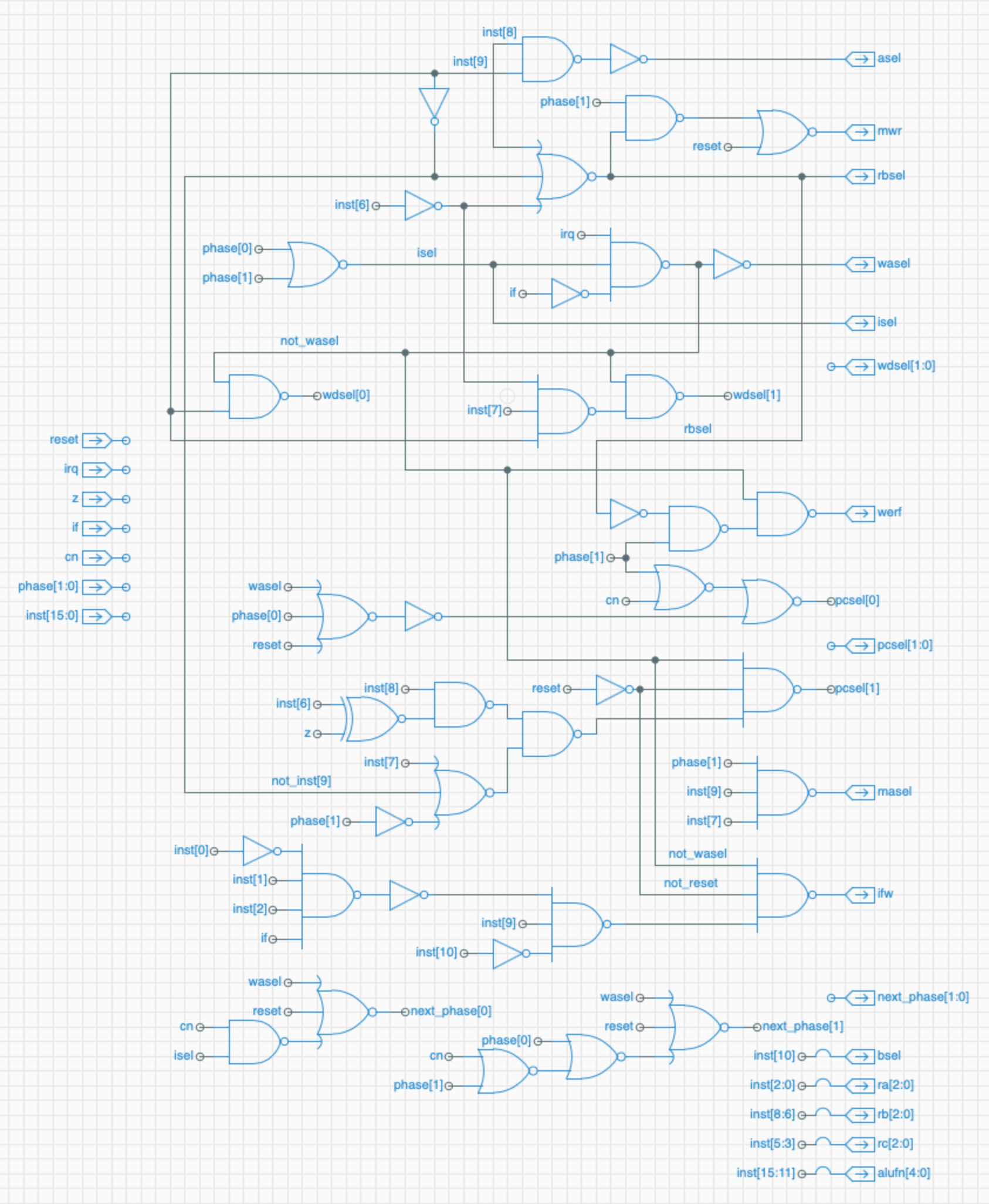
The schematic for the Control Logic is shown below. It simply translates the logic listed above to circuitry. Not shown are the circuits for the flip-flops that store the PHASE and IF status bits. They are similar to the Register Memory Flip-Flops described in an earlier log entry.
To test the implementation, I programmed a Mega2560 to output all possible combinations of inputs, captured all of the outputs, and then compared the output values with calculated values. Here's a photo of the completed board, hooked up to the Mega2650:
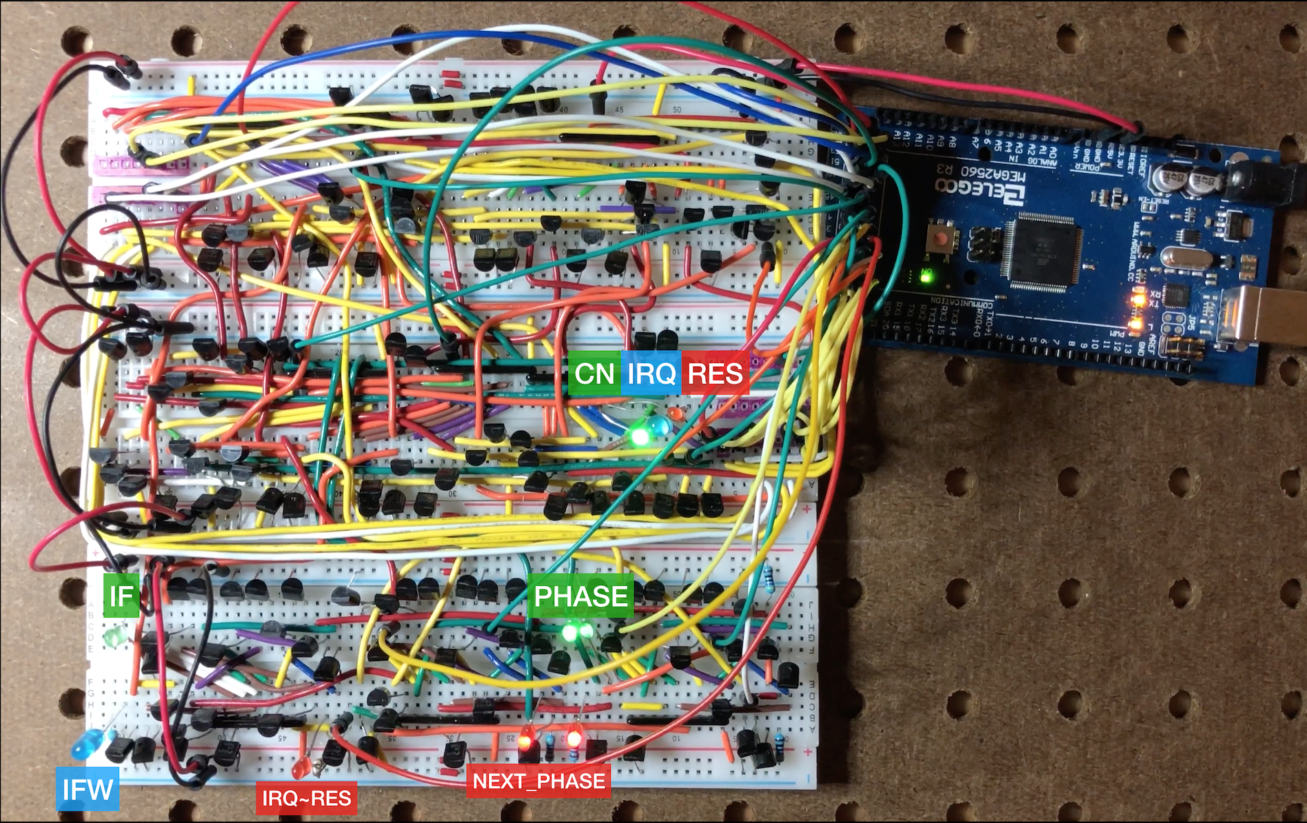
In the following video, you can see the rapidly changing PHASE and NEXT_PHASE signals, as well as a few flashes of IRQ, IFW and IF being stored and cleared. I also show how the Mega sends the Control Logic outputs to the computer for analysis. After a few quick wiring fixes, the boards work as specified. Not too bad for 130 transistors!
Discussions
Become a Hackaday.io Member
Create an account to leave a comment. Already have an account? Log In.