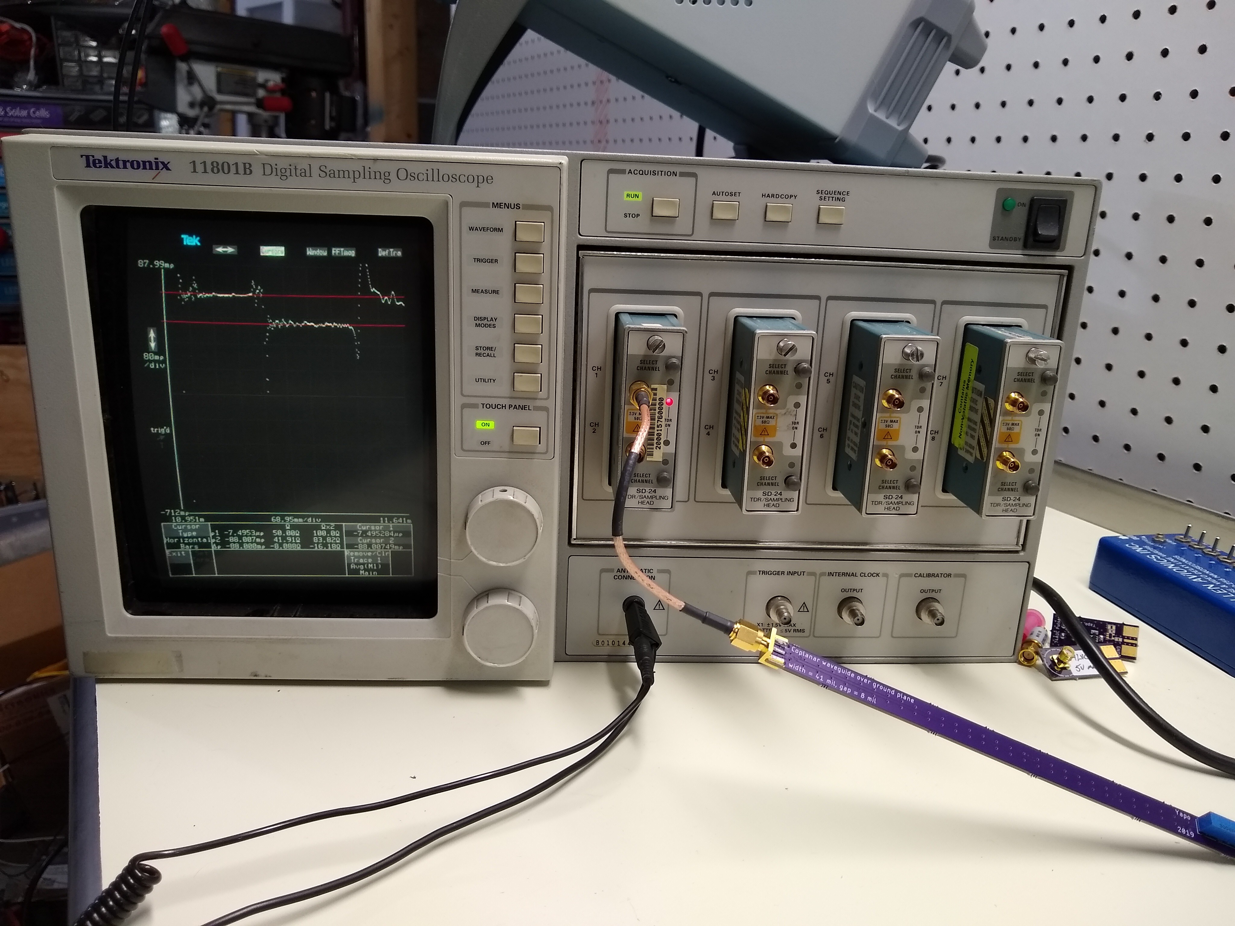
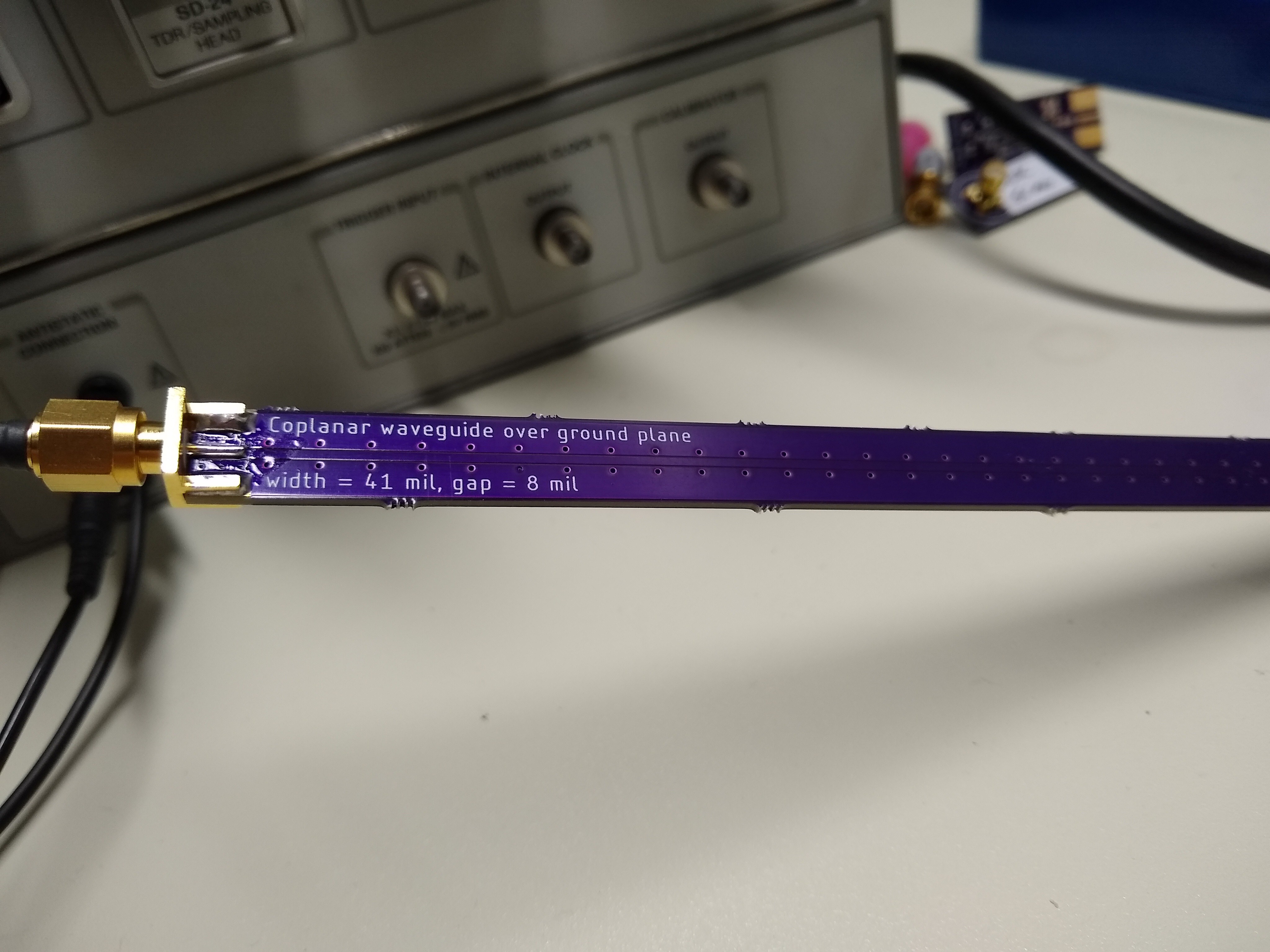
So, I finally found some time to measure the impedance of a test PCB with the new TDR scope. I had made the PCB up a while a go to start validating the proper dimensions for controlled-impedance structures on the OSH Park board stackups, but didn't really have the equipment to measure it accurately until now.

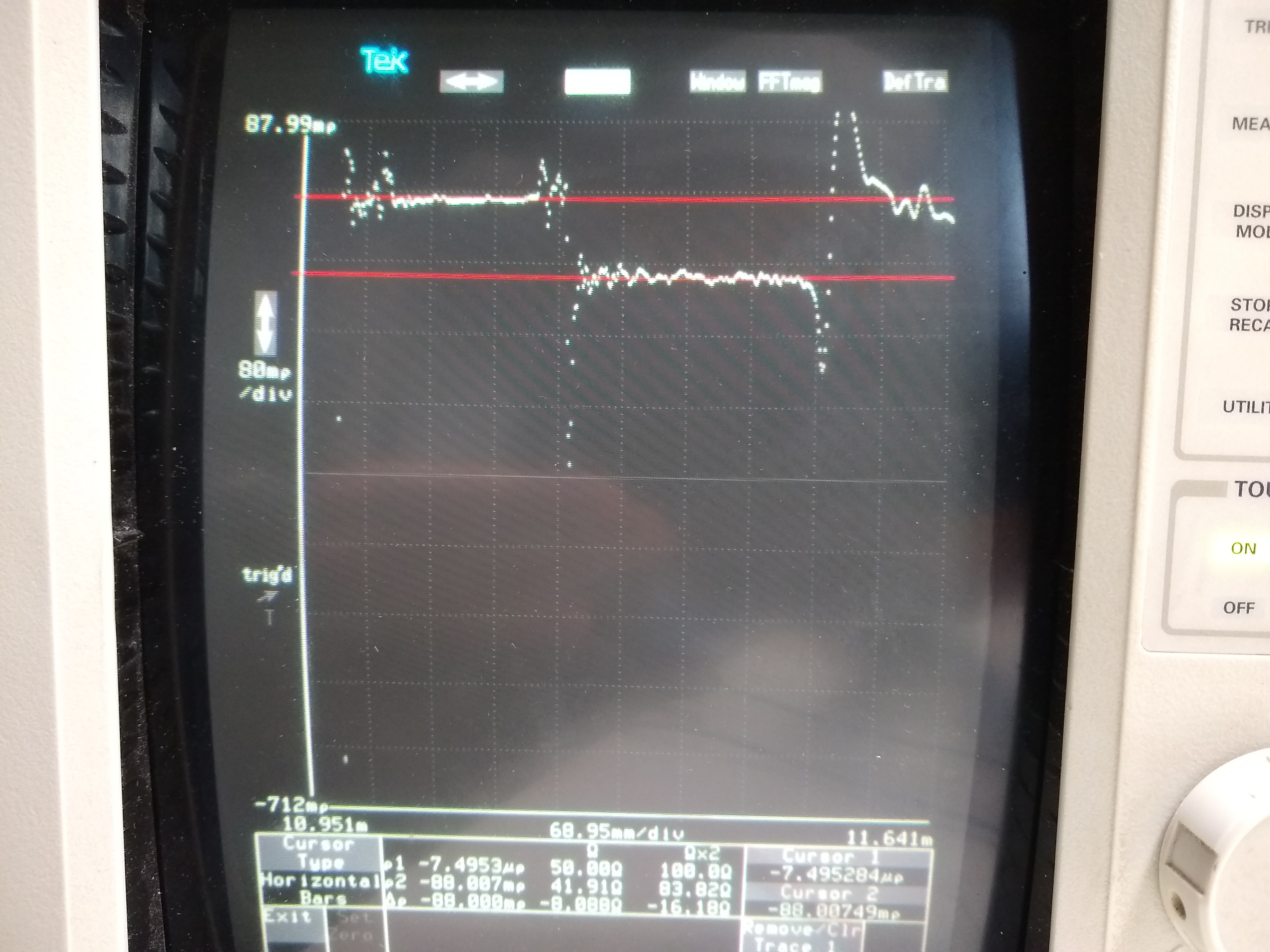
The TDR mode on the scope has direct readout in Ohms (vertical) and either time or length - if you know the velocity factor - on the horizontal. Of course, if you measure the time with the scope, and the physical length with a ruler, you can calculate the velocity factor - which will be my next step.
The measurement results in 50.0 Ohms for the coax jumper, then 41.91 ohms for the PCB trace. It also shows that my PCB footprint for the SMA connector has a nasty reflection. I need to fix that.

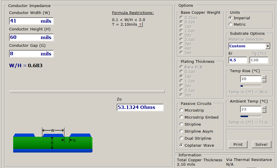
I used an on-line calculator to come up with the dimensions for this coplanar waveguide over ground plane. It gave me a 14 mil trace width and 8 mil spacing for OSH Park's 2-layer stackup. I realize that this is just plain "random" FR4, but I wanted to start with something inexpensive. I also realize that the dielectric will probably change from batch to batch, so I'm not going to chase this one too far. I'm much more interested in the 4-layer stackup on FR408 dielectric.

The thing that bothers me, though, is that Saturn PCB toolkit, for example, says this line should have a 53.2 Ohm impedance.

Calculators are stupid. I need to learn how to use a real electromagnetic simulation program.
Maybe I was right?
I did try to measure this with my own TDR before, but I didn't trust the results. I'll have to go back to my notes and see what I came up with before. I could have dismissed my results if I saw this large discrepancy before.
 Ted Yapo
Discussions
Become a Hackaday.io Member
Create an account to leave a comment. Already have an account? Log In.
https://belfuse.com/resources/cinch-brochures/CCS%20Johnson%20SMA%20HF%20End%20Launch%20App%20Note.pdf
They only show a very thin substrate, but their via fence is quite a bit farther away than the PCB thickness.
FYI: https://www.hasco-inc.com/content/Technical_Articles/Optimizing_Test_Boards.pdf
They show a tapered launch. That should smooth out the impedance transition.
Are you sure? yes | no
Thanks for those links!
I've also been working through TI's app note about signal launch. Who knew there was so much to it :-)
http://www.ti.com/lit/an/snla186/snla186.pdf
Are you sure? yes | no
FYI: for multilayer boards, that picture with the nice straight cyclinder via isn't what your PCB vendor builds. The real one would have annular rings on each internal layers for the plating process even if there were no electrical connections there.
https://kicad-info.s3-us-west-2.amazonaws.com/original/1X/db4127ecaca4262f8a1f6937e360c472252b322c.jpg
Ask for their version of gerber after all their production tweaks.
Back drill to remove excess stub (capactance): https://www.frontline-pcb.com/assets/incam/BackdrillCreation_big.jpg
Are you sure? yes | no
@K.C. Lee Yeah, I know about the rings on internal layers; you can them even in the gerbers Eagle spits out.
I'm not likely to back-drill by hand, and if it isn't offered at the hobbyist-level boards, I probably won't end up designing anything that relies on it, like any other kind of blind or buried vias. Until this stuff becomes mainstream for mere mortals, that is.
Are you sure? yes | no
That EDN article has this statement:
"You can find many online CPWG calculators, but they often fail when the ground-plane gap gets less than approxi-mately 30 to 50% of the trace width be-cause the height of the copper traces on the board becomes a significant factor. It adds more capacitance than the calcula-tors assume. Hence, the lines these cal-culators design have too much capaci-tance, which reduces their impedance to less than 50Ω. The equations date back many years to IC design.The equations in many calculators fall apart because today PCBs differ physi-cally from ICs. The best way to properly design a CPWG on a PCB with a nar-row gap-to-center-trace ratio is to use a full 3-D electromagnetic simulator."
Are you sure? yes | no
Could your ground vias that are right next to the track be an issue?
They could affect the electric field distribution. Normally some of the fields distribute themselves into the FR4 before terminating on the ground plane. The vias (cylinders) provide a shorter path.
http://www.imst.de/coplan/online_manual/images/figure2-12.gif
May be you could try positioning the vias at least 3h distance away - rule of thumb say only 1% of the field at that distance.
This is a case where a 3D field solver would be able to tell you the effects.
Are you sure? yes | no
It's certainly possible that the vias are an issue.
I did find the below EDN article that says a 32mil trace with 6 mil gaps is dead-nuts 50-ohm, supposedly tested (with some kind of 62 mil FR4). They use vias close to the track. But, no soldermask. I haven't had one like this fabbed yet, but I'm going to include one on the next test board. The online calculators put this 32/6 structure right at 50 ohms, like my 41/8 version. So, I'm thinking it's soldermask, which remains in the gap even after I sanded it off the copper.
https://www.edn.com/design/components-and-packaging/4363897/Make-a-quick-turnaround-PCB-for-RF-parts
Are you sure? yes | no
You could try drilling out a few of those vias with a larger drill bit. If they show a different impedance, then that's the answer. You got a TDR... :P
BTW: The vias in the article are a bit farther away - probably closer to 2h.
Are you sure? yes | no
Wow, you got yourself a pretty boatanchor :-P
Are you sure? yes | no
28 kg and it takes up most of my bench, but it's fast enough - for the moment :-)
I found in the menus last night it has over 75,000 operating hours. Still works fine. They built them right back then.
Are you sure? yes | no
It's the same generation/build as my 11302 :-D what a nightmare...
Are you sure? yes | no
Usually you would talk to your production PCB vendor as they deal with controlled impedance. They know their process best. They would typically tweak your gerber files - track width to adjust them to +/- 10% of the required values for production volumes. Include a calibration coupon - test traces for QC.
For accurate work, you want to use a 2D or 3D field solver (finite elements) as most of those quick calculators make a lot of assumptions. You want to read the fine prints on the conditions of these approximations and see if you are near the limits.
Are you sure? yes | no
Yes, that's how I understand the process for manufacturing. For hobbyist/small-scale, though, I think it makes sense to know how accurate and repeatable you can get with a common, known service.
The 4-layer boards from OSH Park on FR408 should be good enough to tabulate some tested geometries for various structures and impedances. If I could consult such a table myself, I never would have started down this road, but now, I feel like it really should be done.
I get the field solver thing. Looking into openEMS and MEEP now. They're just both a real PITA to install.
Are you sure? yes | no
Here is the part that "Open Source Hardware" distribution model is broken - expecting turn key ready to manufacturing. Making hardware requires extra work and tweaks to match your manufacturing.
You can't just blindly copy/paste gerbers and expect the PCB to be portable across all the board shops and assume that they all have same capabilities, electrical characteristics and manufacturability.
Are you sure? yes | no
Let me ask you this: are PCB vendors tweaking track widths on a per-batch basis, or do they have their processes dialed-in enough to adjust the design once, then manufacture it repeatably?
Are you sure? yes | no
I don't know the answer. I talked to them one time and they know the dielectric constant and can make good control impedance. I would also assume that they have automated the process for tweaking track width.
They probably know their material (FR4 dielectric, prepreg, soldermask) from their suppliers and their own process (under etch, plating thickness) well enough.
I would assume that they would do it on batches among the different customers with similar Tg material, thickness. If there are material changes from suppliers, then they might need to tweaks it.
Are you sure? yes | no
Perhaps in the calculations should take into account the influence of the solder mask?
Are you sure? yes | no
Yes, they certainly should. This would account for a drop in impedance, but I would expect it to be relatively small, maybe an ohm or two as a guess. But, just a guess.
Are you sure? yes | no
I sanded off the solder mask. Impedance went up by a little less than 1 Ohm.
Are you sure? yes | no
I am not sure of my reasoning which I will give below. Last time I held a book on electrodynamics in my hands more than 25 years ago :-)
You use the Coplanar Waveguide, in this case most of the energy of the electromagnetic wave is concentrated in the gap G (8mils). How accurately it is made, what it is filled with - the line resistance will depend on it. Vias in the immediate vicinity of the line can also make their own adjustments.
It seems to me that you need to change the design of your line so that the spread of technological parameters will have less impact on the result.
Once again, I have no experience in this matter. And the reason really can be in random FR4.
Are you sure? yes | no
@Serge yes, the gap is very important. It was suggested that I measure it, and I gave it my best shot with the microscope and counting pixels method. I came up with 39 mils for the track and 7.2 mils for the gaps. Plugging these values back into the various calculators doesn't account for the difference.
As for the filling, I was able to sand the soldermask off the copper to test the effect (less than 1 Ohm), but it probably remains inside the gap. You may have found the problem there - soldermask has a high Er, and would push the impedance lower.
I tried a bunch of chemical methods to remove the soldermask, but none worked. I'll have to see if there's a way to get it out of there without waiting for new boards.
Yeah, I get that this could just be random FR4, but I'm not ready to concede that yet.
Are you sure? yes | no
https://electronics.stackexchange.com/questions/39834/placement-of-vias-to-connect-ground-planes
Are you sure? yes | no
Hi Ted, I'm just coming up to speed with openEMS. If you use pcbmodelgen (on Linux), you can import straight from kicad pcb files. Maybe it is the kind of thing that will help you "sim-b4-u-fab".
Are you sure? yes | no
That's a good suggestion.
I've glanced at openEMS before, but since I kind of broke up with matlab/octave, I really didn't want to go back, and the python interface on openEMS doesn't seem to be fully baked yet. But, some googling shows there's a hyperlynx output script for Eagle, them hyp2mat can convert that for openEMS. It's worth a shot.
I'm an Eagle type, you know.
Are you sure? yes | no