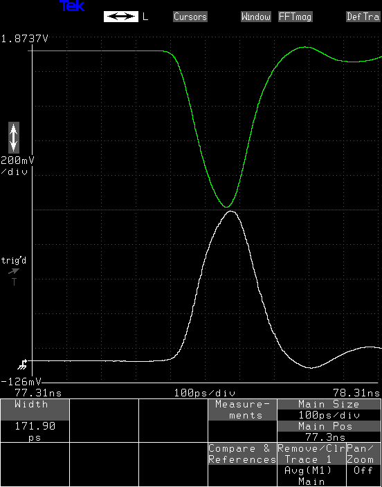
This time around, it's a differential strobe pulse generator designed around two laser diode driver ICs. The SY88932L is intended for driving fiber-optic lasers at up to 4.25 Gbps. The key thing I wanted to test with this board was creating short pulses with clip lines. Using this technique, I was able to generate strobe pulses of 172 ps width. That's narrow enough for a 2 GHz sampling head.
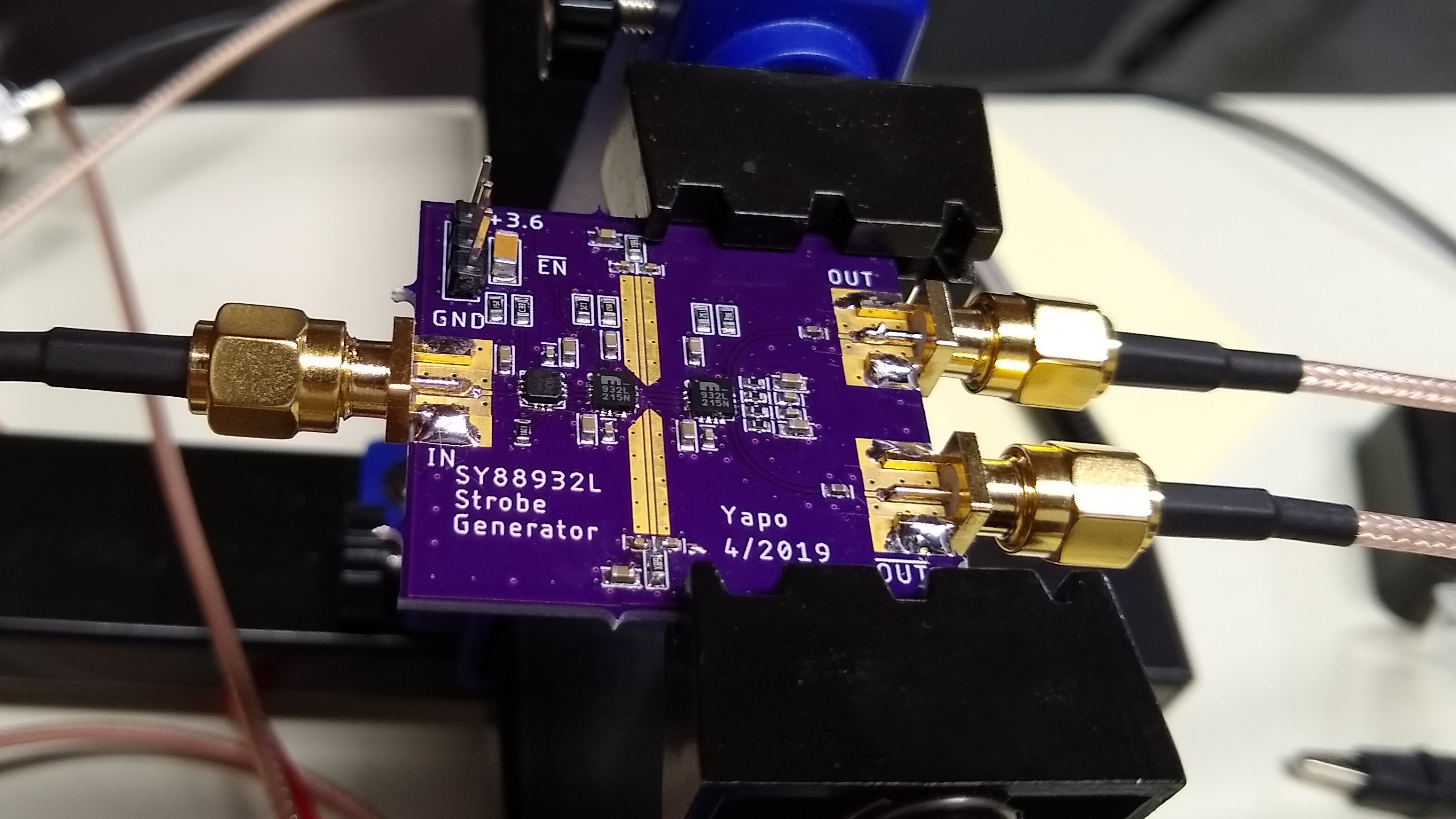
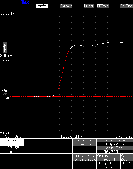
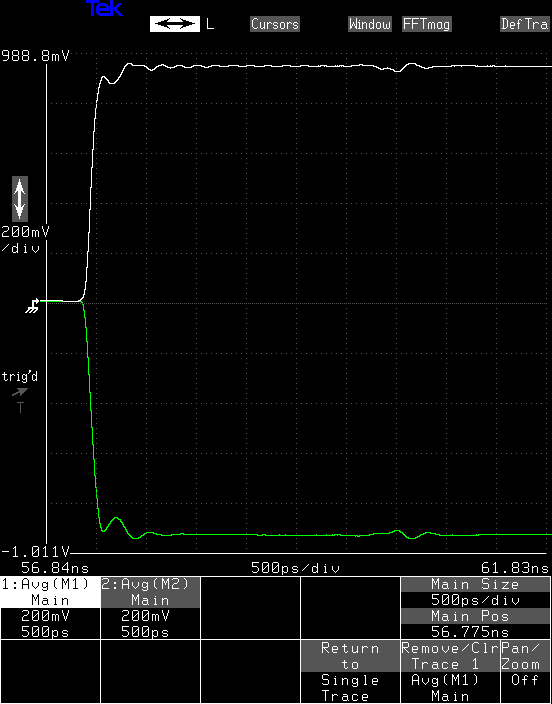
The laser driver claims typical rise and fall times of 65 ps (20%-80%), and I've measured around 100 ps (10%-90%). I made a simpler breakout to test just the SY88932L, but due to a supply chain snafu, I ended up having to remove the part from that PCB to populate this one.
SY88932L
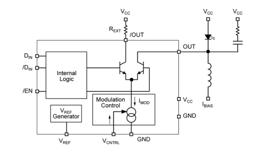
I like this part because the logic is simple and the outputs are open-collectors. Some laser diode drivers are internally terminated with resistors, or worse, some kind of active bullshit which interferes with using them as general-purpose drivers. I don't know how far above Vcc you can push the outputs - the datasheet claims they can only go to Vcc, but I'm guessing you could probably go a few hundred mV above before any protection diodes kicked in. I'd really love if these were just raw open collectors, but I don't think so. At some point, I'm going to have to add some really fast external transistors to boost the output swing. But for these early tests, this part works OK.
Strobe Generator Circuit
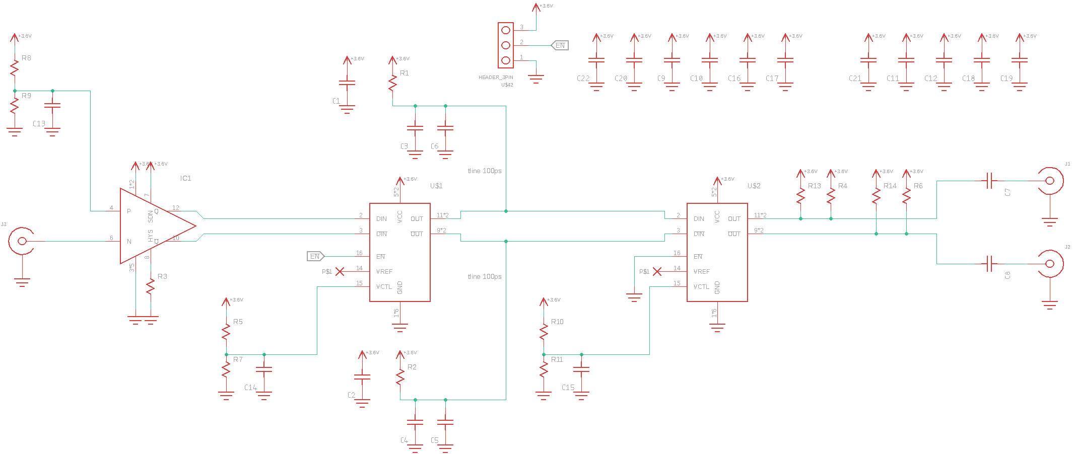
Here's the 172 ps strobe generator. The input is converted by an ADCMP607 comparator. This part has a single-resistor-controlled hysteresis level and CML outputs which can drive the other ICs directly. I've chosen the input threshold to suit the clock output of the 11801 sampling scope for convenient triggering. There are two SY88932L's on the board: the first one generates short differential pulses using clip lines, and the second is used as an output driver. This really is just a prototype/breakout PCB. It sucks when you have to spin a 4-layer PCB just for one test, but this isn't the kind of stuff you can do on a solderless breadboard :-) The clip lines are just marked in text annotations; to Eagle, they're just normal traces. More on the clip lines below.
PCB
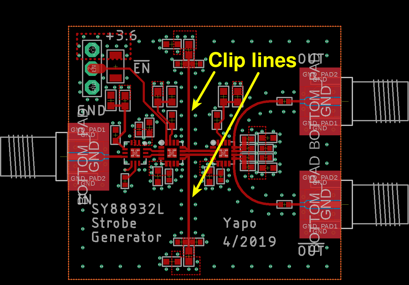
This is the PCB, with the clip lines annotated. There's an LTspice simulation further down the page that shows more about how this works, but in a nutshell, transmission lines with shorted ends are used to define the pulse width. A current pulse into the open end of the line can only exist for as long as the pulse takes to travel the length of the line, reflect off the end, and return to cancel the original pulse. Since the CML signals are differential, two identical lines are required. In this case, the lines are just made with coplanar waveguide traces on the top of the PCB. The advantage of this technique is that the timing is easily controlled and stable.
Tektronix used this technique to control pulses generated by step recovery diodes in their 1960s-era oscilloscope sampling heads. I found one for $30 on ebay so I can do a teardown - schematics are available, but they don't tell the whole story *at all*.
LTspice Simulation
LTspice has a transmission line component that makes modeling the important part of this circuit easy. The transmission lines on the left are the clip lines, while those on the right are just the connecting traces between the two ICs. The open-collector outputs of the laser driver are modeled with current sources. There's an internal 50-ohm termination (right) inside the driver's inputs. The clip line is AC terminated at the resting-state voltage of each line by a 50-Ohm resistor and shunt capacitor. This causes an inverted reflection from the end of the line.
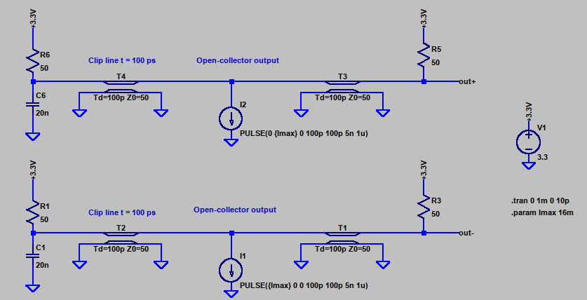
The output of the simulation shows what's going on. One of the input current pulses is shown in the top (red trace). The leading edge of the pulse switches the output at first, but eventually, the reflection arrives to cancel it out. On the trailing edge of the input pulse, short output pulses are also generated, but since their excursion is in the same direction as the resting differential state of the lines, they have no effect. So, the net result is a short pulse just on the rising edge of the current pulses.

Output Measurements
The measured pulse width is 172 ps. You can't go any shorter without reducing the pulse amplitude because the edges aren't fast enough. In fact, I suspect you could get a little more amplitude by extending the clip lines. But, this would require a board spin, and this was just a proof-of-concept. This is twice as fast as my previous strobe board, which achieved a 348 ps pulse.
The clip lines are 465 mils long. OSH Park 4-layer boards use an FR408 substrate with an Er ~ 3.66, so signals travel at 162 ps per inch. The clip lines should have a 75 ps one-way, or 150 ps round-trip time. So, the output width seems to be about right. I'm not sure what the scope was using as the high reference when doing the width estimation, either. I could dig more into it I guess, but I don't really think there's any mystery here.
At a longer timescale, you can see some reflections. The first set, right at the end of the strobe, are probably due to my bad SMA-connector footprint, $0.20 eBay SMA connectors, and poor-quality cable. The wiggles 3 ns later are caused by reflections from the interface of my cheap cables and the scope input. The connecting cables are around 30 cm long, and at a velocity factor of 0.66, a pulse takes around 3 ns to traverse the cable down and back.
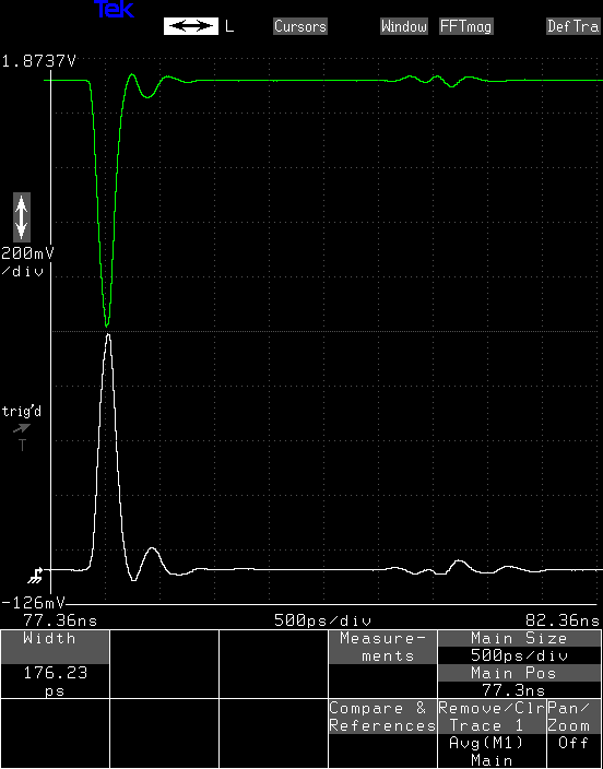
The pulse width and shape seem pretty good. If I can find faster open-collector drivers, I think this method could be useful for even shorter pulses. The problem is that IC designers are always trying to make everyone's life easier, so keep adding crap to laser diode drivers that make it easy to design network adapters, but complicate using them for general-purpose drivers.
The amplitude is too small, so the PCB I just sent out has a differential pair of 12 GHz transistors at the output to increase the compliance range of the current sources. I really didn't want to go there, but it looks unavoidable at this point. Maybe it won't be that bad.
SY88932L Edge
Just for reference, here's the edge of the driver by itself. This was on the previous PCB I had to depopulate. I think the wiggles at the top of the step are again due to cheap SMA connectors and bad footprints. I'm working on that,
And here's a shot of both outputs at a longer timescale. I really need to fix those SMA launches.
 Ted Yapo
Discussions
Become a Hackaday.io Member
Create an account to leave a comment. Already have an account? Log In.
FYI: Picosecond Pulse Generation Techniques & Pulser Capabilities James R. Andrews
https://kh6htv.files.wordpress.com/2015/11/an-19-pulse-gen-techniques.pdf
Are you sure? yes | no
Thanks! I have a decent collection of their app notes, which are a pain to find now since Tektronix bought them, merged the web sites, and broke everyone's links. That's the thing I hate most about M&A in the electronics space.
Are you sure? yes | no