 Trevor Johansen Aase
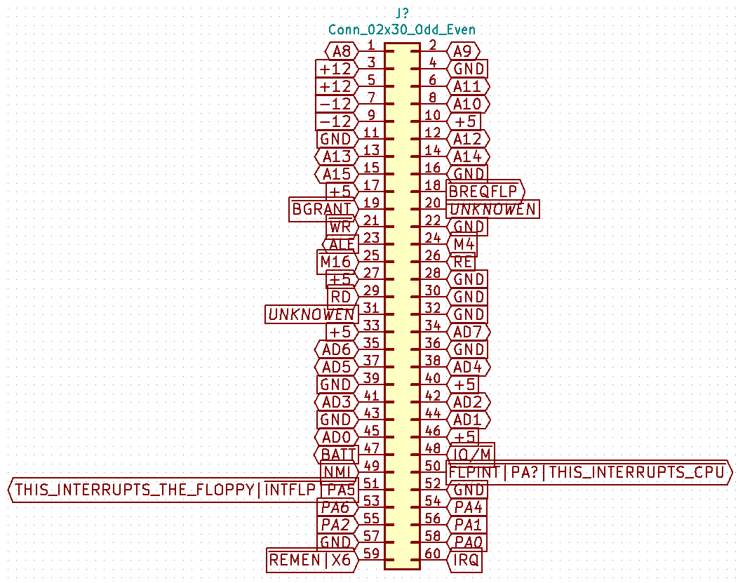
Here is what I have been able to piece together of the J1 system bus. AD0-7 and A8-A15 are the multiplexed address and data pins. You can address 64k max directly through the system bus. RD, WR, ALE, IO/M, NMI, IRQ are z80 style pins but there are a few weird unknowns.
The PA0..PA6 are the peripheral select pins after some IO decoding and share interrupts between boards. I only decoded the two.
These pins are from the 4951C drawings. Seeing as the same floppy board is in both machine I would expect the pinout to be the same. Hopefully?
BGRANT
BREQFLP (Bus Request Floppy I assume)
RAMEN / X6
RE
M4
M16
Pin 31
Pin 20
Discussions
Become a Hackaday.io Member
Create an account to leave a comment. Already have an account? Log In.