 Trevor Johansen Aase
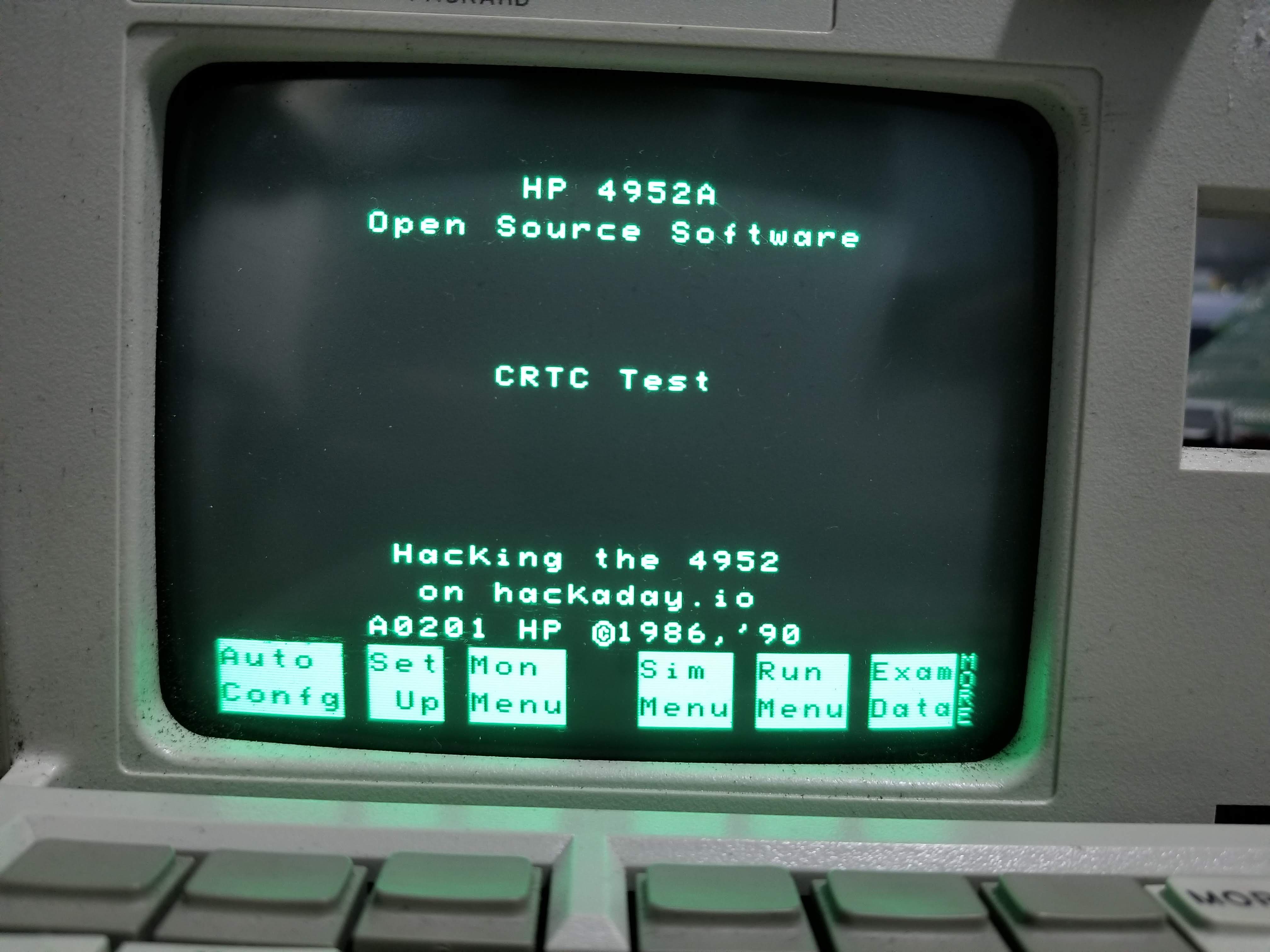
So I figured an interesting place to poke around on was the CRTC (MC6845) as it was well documented.
First I had to put the logic analyzer on the J1 bus to see what IO address was being output. This was challenging as my pinout is not exactly correct. In the end I discovered:
    _crtc_wr: equ 0a0h
    _crtc_wd: equ 0a1h
    _crtc_rr: equ 0a2h
    _crtc_rd: equ 0a3h
So I wrote a very terrible asm program that uses the keyboard to modify the 10 registers of interest in the CRTC.
Stock CRTC timing is 32 x 16 @ ~60hz:
I can eek 35 x 32 @ ~28hz:
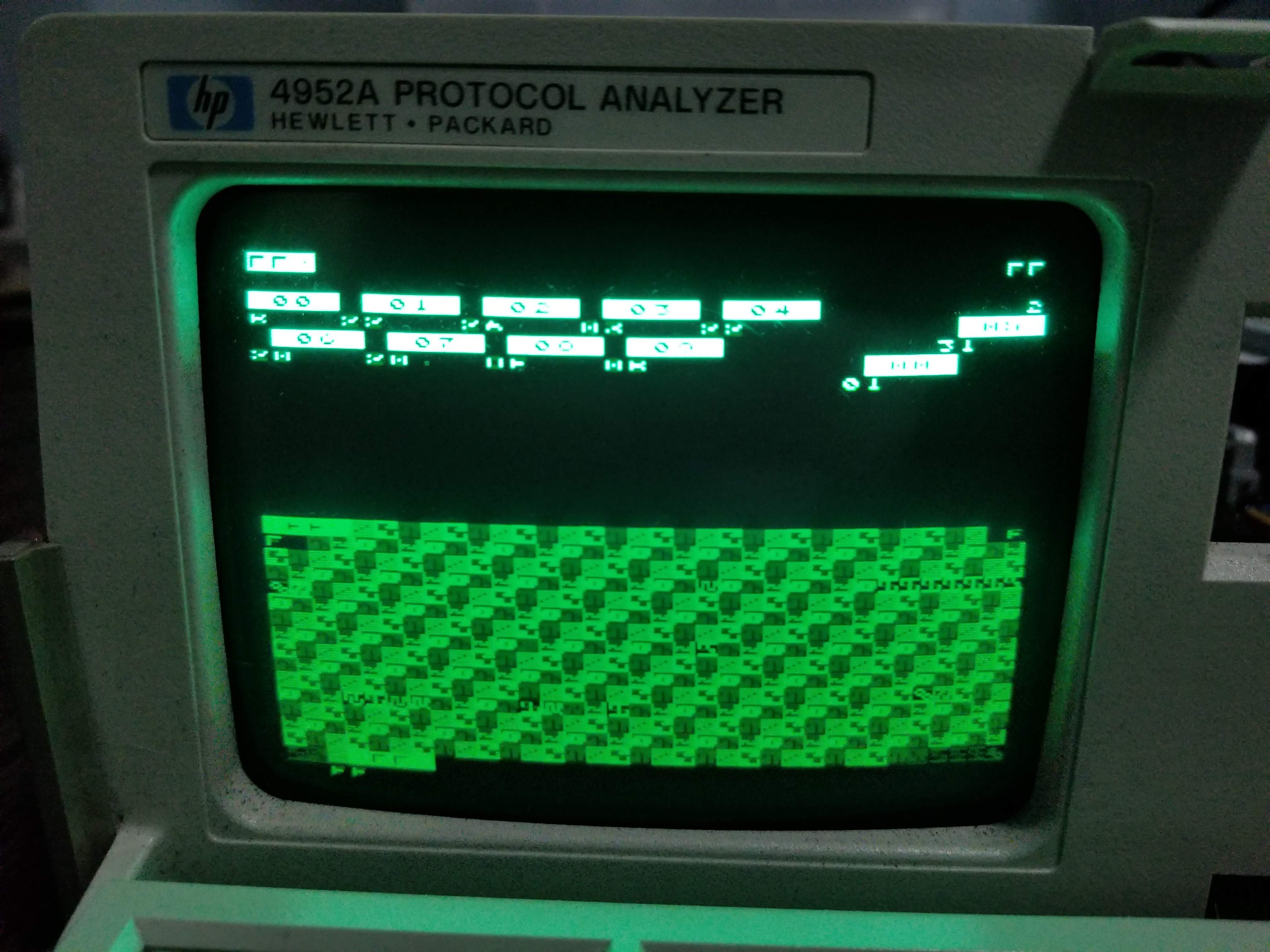
This as it turns out is not particularly useful as you wrap the address space of the memory's ram and start to display from the beginning again. Also the 28hz is a very noticeable screen flicker. All the garbage on the bottom half of the screen is exactly that, garbage in RAM as the screen is never meant to display that address space.
So an interesting thing to poke at. Maybe when the entire system rom is replaced a larger screen format can be useful. For now, not so much.
Discussions
Become a Hackaday.io Member
Create an account to leave a comment. Already have an account? Log In.