 Trevor Johansen Aase
Here is a picture of the main board.
The grey 2x20 header goes to the interface pod. Looks like a dedicated z80 just to handle that with a dedicated PIO chip. The Toshiba chip is also a z80 and I am thinking it handles the UI. Grey cable on top is the bus link to the daughter boards.
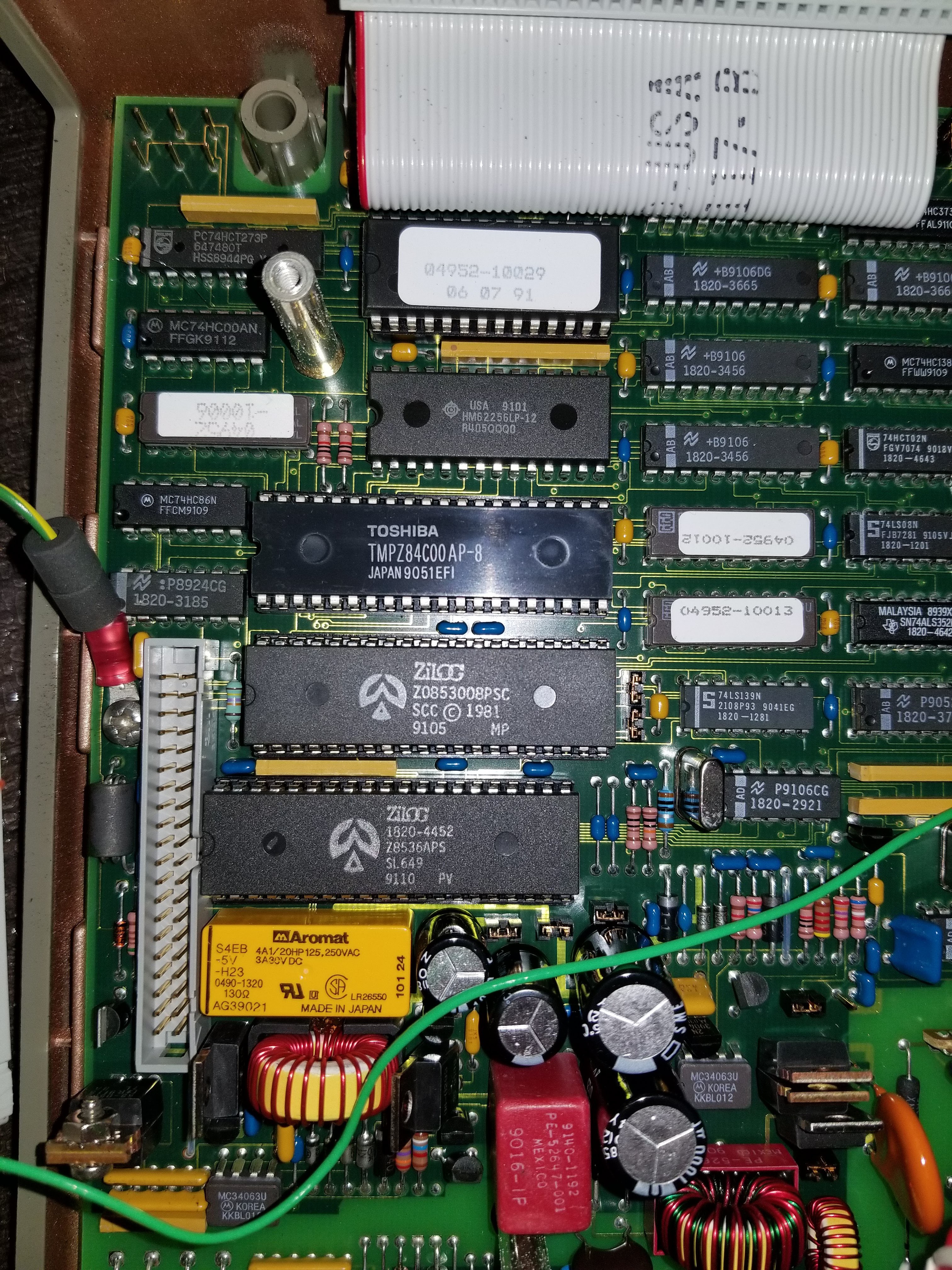
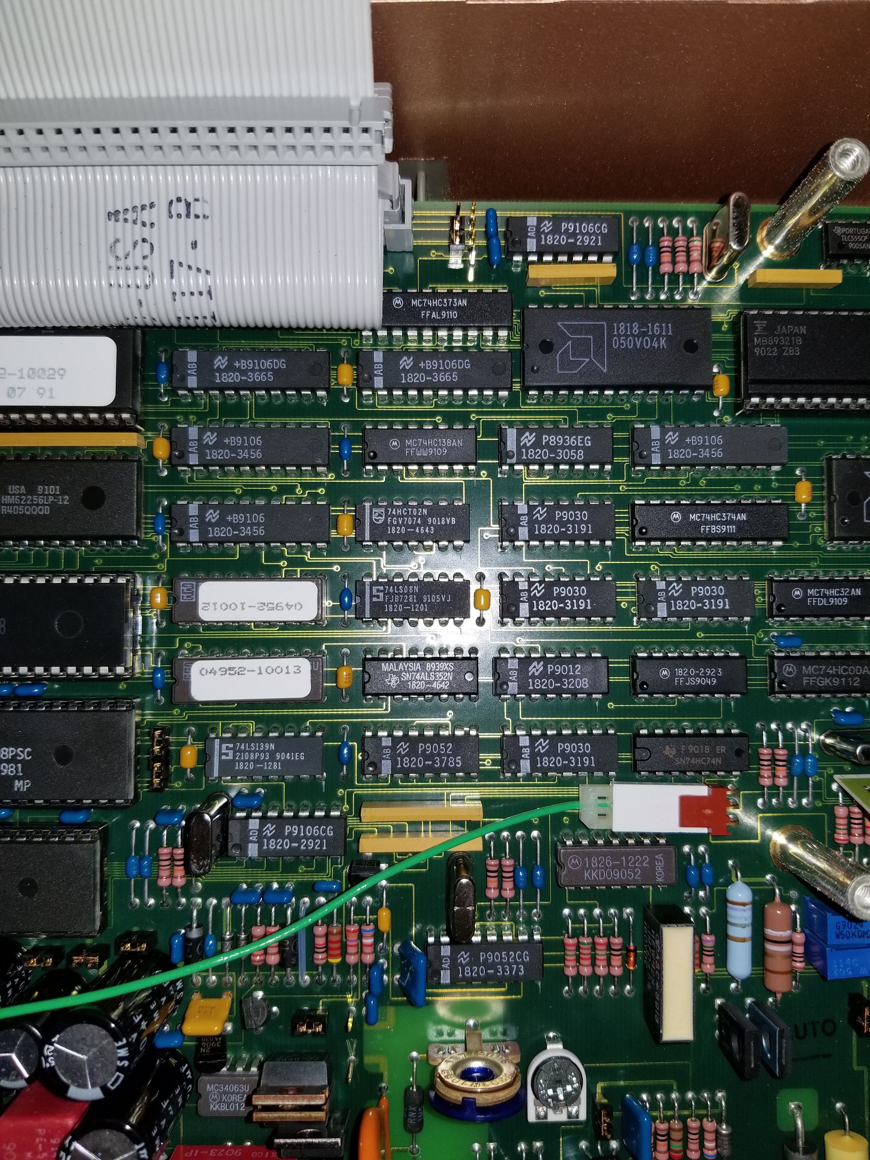
Lots of unknown chips in here. By position its likely the video driver logic. Single green wire goes to the BNC for Video 170.
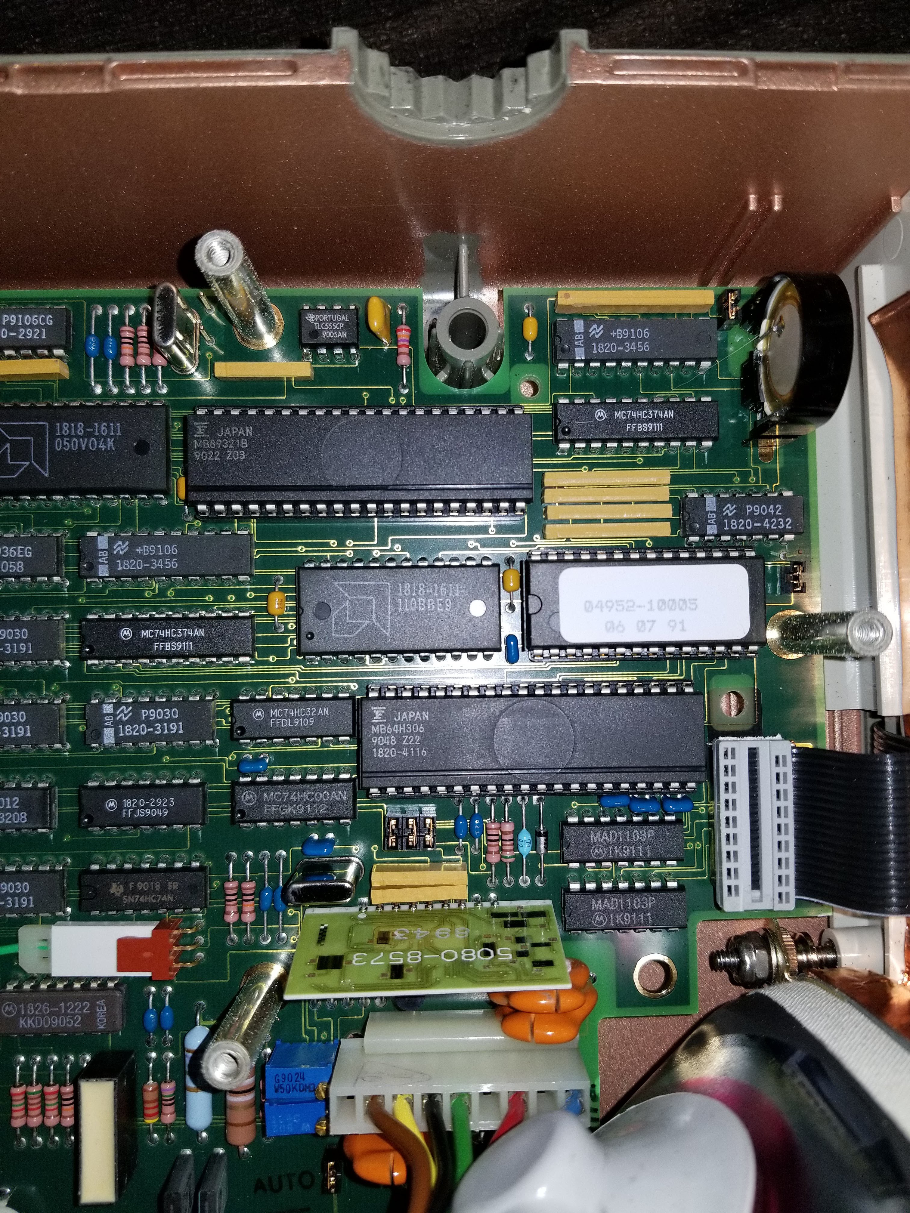
Big chip on the bottom is a FUJITSU MB89321BP CRT raster controller. The similar one above I could not find anything on. The vertical PCB is likely the deflection transistors for easy replacement. The grey DIP ribbon cable is the keyboard.
Discussions
Become a Hackaday.io Member
Create an account to leave a comment. Already have an account? Log In.