Trevor Johansen Aase
-
Floppy Controller
02/18/2019 at 21:44 • 3 commentsx86 ASM is not a pretty sight. x86 addressing sucks.
So I was banging my head on the wall with reverse engineering the main memory board when I figured "Hey, I have the full schematic of the floppy board, why not just use it as the main processor instead?!" The video hardware is accessible via the J1 backplane so it sure is possible.
I dumped the 256kb rom and was immediately confused. I have never done x86 ASM and specifically chose z80 because the mnemonics make clear sense. The addressing is also linear and straight forward. The x86 machines of the past use a crazy offset system that you were forced to use. Here is a HaD writeup on how it works.
So this board boots to 0xFFFF0 but a 256kb rom is only 0x7FFF so essentially that means the reset instruction is at 0x7FF0. That instruction is EA 65 A4 00 F0 or Jump Far (0xA465 Left shift x4) + 0xF000 which is JMP 0xB3650. Once again we can only address 256kb so and that with 0x7FFF to get an effective JMP 0x3650. Now why is the world didn't they just do EA 00 00 50 36 or even EA 00 F8 50 36?!
EDIT: Upon reviewing the schematics I forgot how the memory was mapped and assumed ROM was at 0x00 like the z80. RAM is 0x0000:0x7FFF and ROM is 0xC0000:0xC7FFF and due to ignoring A15..A17 it repeats at 0xC8000, 0xD0000, 0xD8000, 0xE0000, 0xE8000, 0xF0000, 0xF8000. JMP 0xB3635 still makes no since but it's closer at least.
Well 0x3650 does drop us into a string of subroutines but they mean nothing to me as its all just ex ax xi over and over again. Cutter and IDA are not overly helpful as they can not extract that is code and what is data.
Copy protection or data obfuscation by HP:
I find patches of code that are meaningless and are never called. in the 80c88 there are opcodes that don't exist x86 OpCodes You get a 00 60 00 which is absolutely nothing and does nothing. As its a ROM its not even a placeholder bit for a local variable. I swear that the guys at HP have a random number generator that fills a 256kb file and they or it with their code so all blank spaces are filled with complete garbage for obfuscation.
-
Getting Programs To Your 4952
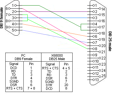
01/27/2019 at 02:14 • 2 commentsGet a real serial port or a FTDI Chipi-X line level serial adaptor.
Also get a DB9 to DB25 adaptor or make your own. Pinout:
![]()
Get the DOS utilities disk HERE and extract "495XPCUtil_D1.zip" to a DOS directory.
Download / apt-get DosBox
Create a dosbox.conf file in the DOS directory:
[serial]
serial1=directserial realport:ttyUSB0

[autoexec]
mount C "."
C:
dir
This will automatically load the current folder as C and display it to you so you know it's mounted.
The serial port may be different for you, I'm on linux with an FTDI adaptor so ttyUSB0 for me.
Now all you need to do is run 5XREMOTE.EXE and you can communicate with your 4952.
1 - Run '5XREMOTE.EXE'
2 - Enter 9600 as the Baud Rate
3 - 'Delete Slave's Application Module'
4 - 'Download Application Module'
5 - 'Execute Slaves Application Module'
If you did a cold boot then you can skip step 3, otherwise you need to delete the old app before you can upload a new one.
NOTE: On linux machine dosbox IS case sensitive. DOS is not case sensitive so its a bit of an annoying issue. When you load your app the interface only allows upper case names and it provides the .APP for you. You need to make sure your programs are uppercase as well as the extention or else it won't find them.
-
Playing With CRTC Timing
01/27/2019 at 01:44 • 0 commentsSo I figured an interesting place to poke around on was the CRTC (MC6845) as it was well documented.
First I had to put the logic analyzer on the J1 bus to see what IO address was being output. This was challenging as my pinout is not exactly correct. In the end I discovered:
    _crtc_wr: equ 0a0h
    _crtc_wd: equ 0a1h
    _crtc_rr: equ 0a2h
    _crtc_rd: equ 0a3h
So I wrote a very terrible asm program that uses the keyboard to modify the 10 registers of interest in the CRTC.
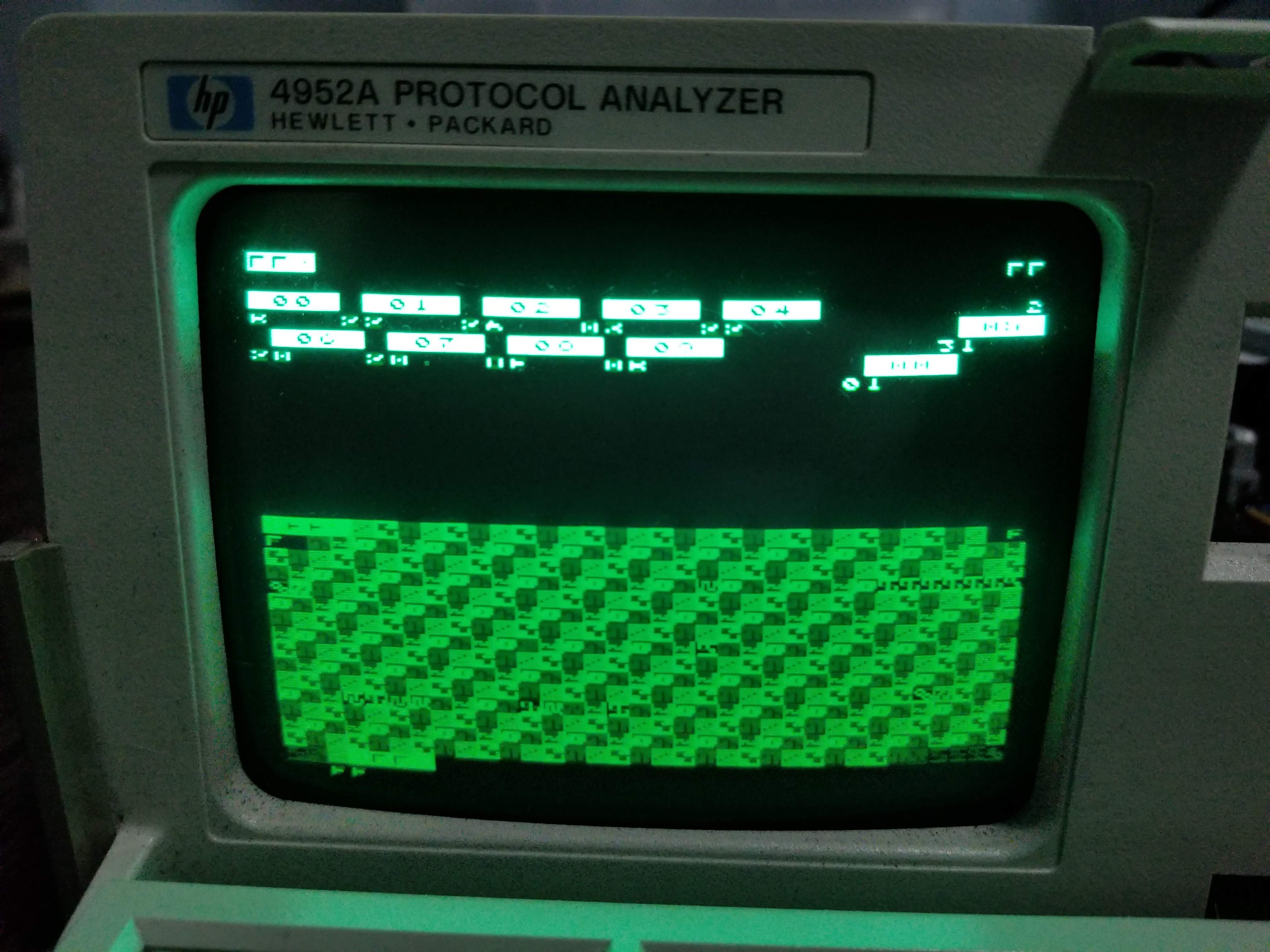
Stock CRTC timing is 32 x 16 @ ~60hz:
![]()
I can eek 35 x 32 @ ~28hz:
![]()
This as it turns out is not particularly useful as you wrap the address space of the memory's ram and start to display from the beginning again. Also the 28hz is a very noticeable screen flicker. All the garbage on the bottom half of the screen is exactly that, garbage in RAM as the screen is never meant to display that address space.
So an interesting thing to poke at. Maybe when the entire system rom is replaced a larger screen format can be useful. For now, not so much.
-
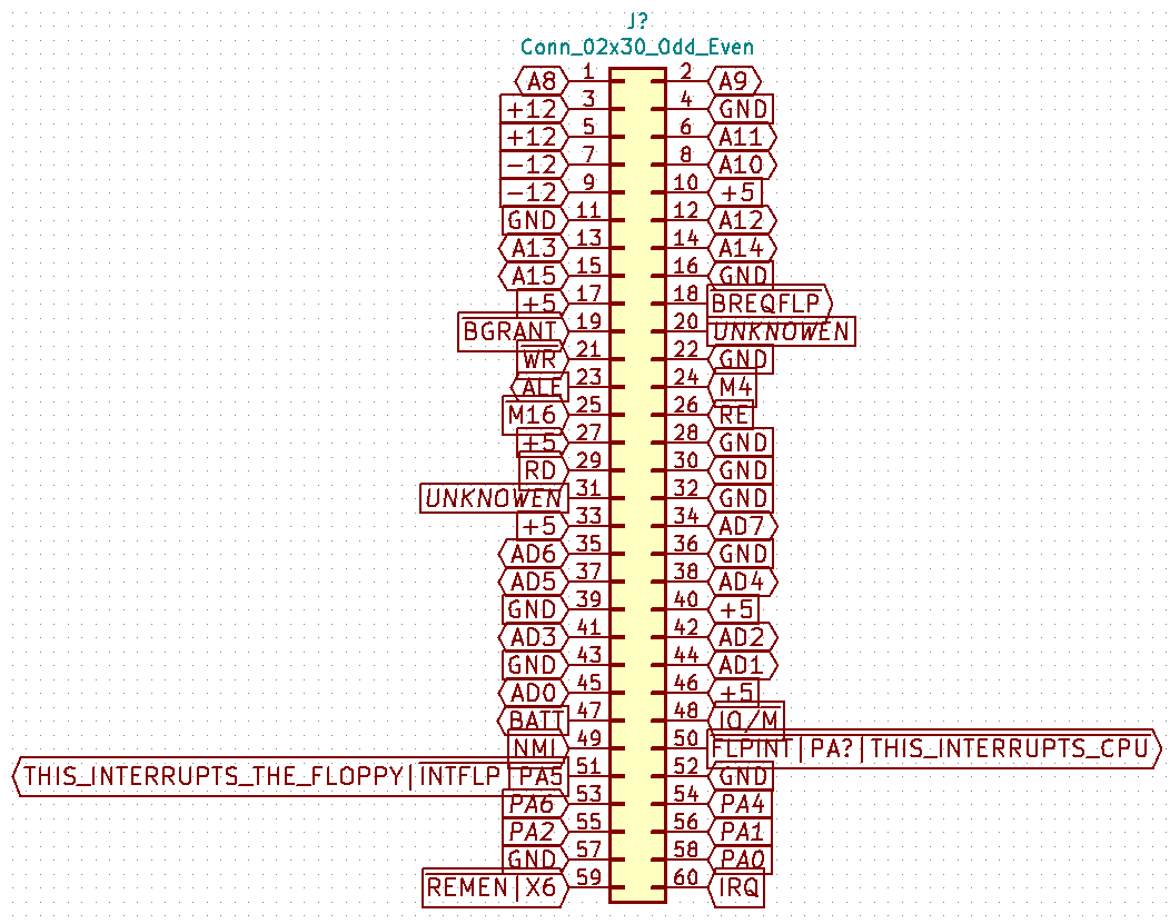
System Bus J1 Pinout
12/31/2018 at 23:29 • 0 comments![]()
Here is what I have been able to piece together of the J1 system bus. AD0-7 and A8-A15 are the multiplexed address and data pins. You can address 64k max directly through the system bus. RD, WR, ALE, IO/M, NMI, IRQ are z80 style pins but there are a few weird unknowns.
The PA0..PA6 are the peripheral select pins after some IO decoding and share interrupts between boards. I only decoded the two.
These pins are from the 4951C drawings. Seeing as the same floppy board is in both machine I would expect the pinout to be the same. Hopefully?
BGRANT
BREQFLP (Bus Request Floppy I assume)
RAMEN / X6
RE
M4
M16
Pin 31
Pin 20
-
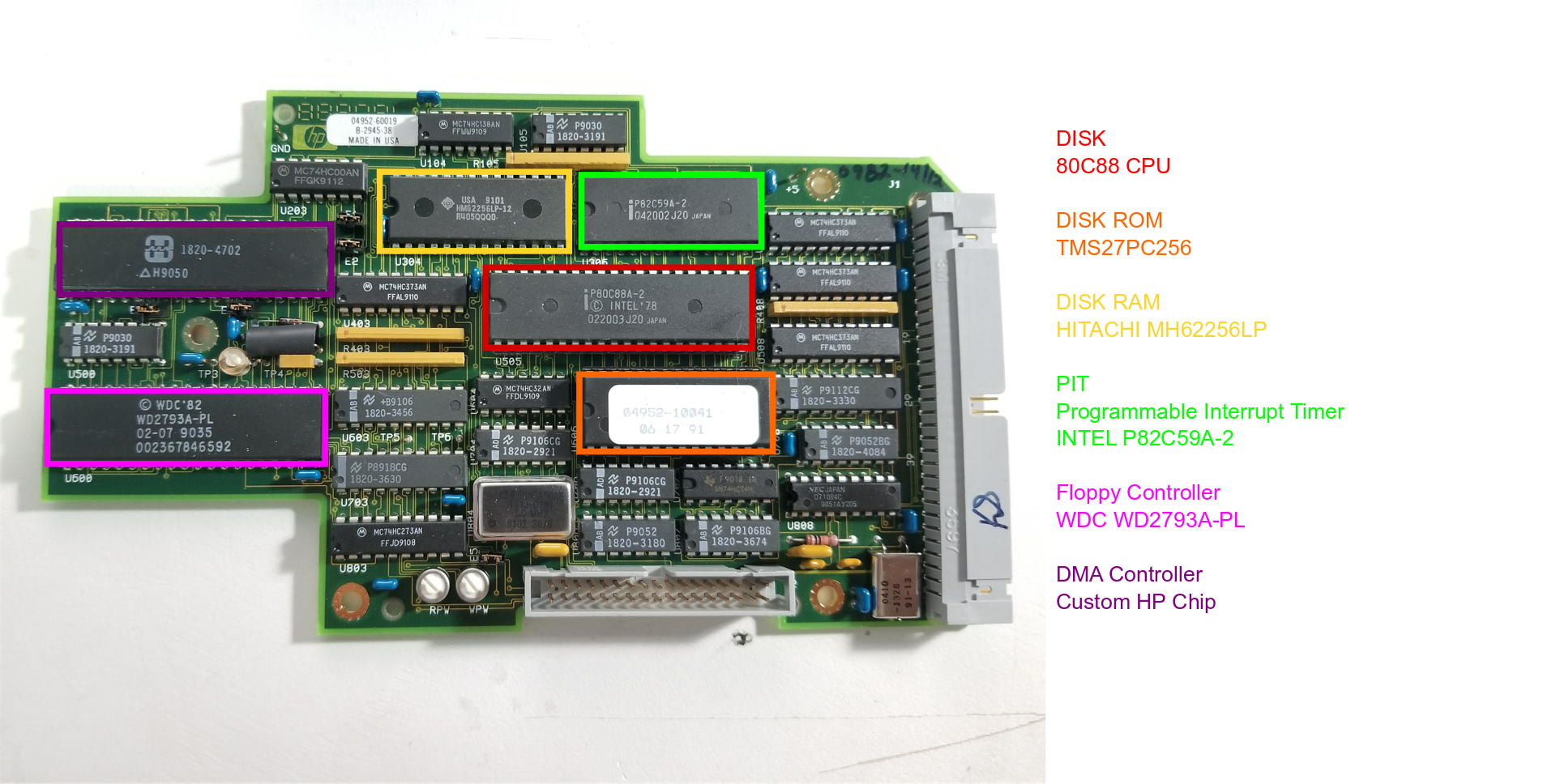
Disk Controller Breakdown
12/31/2018 at 23:06 • 0 comments![]()
This is a simple little board. Exactly the same as in the 4951C so I have full schematics. This gave me the initial system bus J1 pinout.
Nothing interesting to note other than the fact that the entire card is essentially an SBC. Full 8088 processor with 32k RAM & ROM. The typical WDC floppy controller. There is a custom DMA controller and PIT interrupt generator.
The manual says that this board will load a disk transparently into memory. I assume they mean the "file" that contains the bus data only as there is not enough system ram.
-
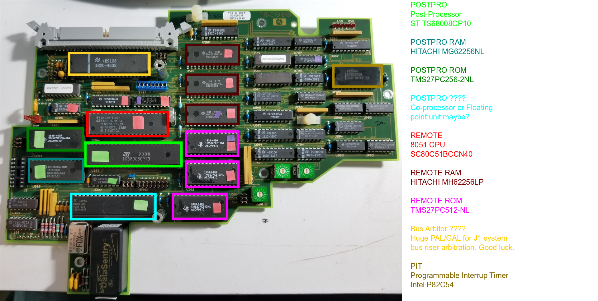
Memory Board Breakdown
12/31/2018 at 22:59 • 0 comments![]()
** Very Confused Point **
I have removed the PIO, Zilinx z80, Toshiba z80, toshibas ROM, Postprocessor CPU/RAM/coprocessor, the 8051 AND the disk board is not plugged in. THERE ARE NO MORE PROCESSORS IN THIS THING. WHY DOES IT STILL WORK?!
All the self test fail of course but the hardware tests run an the main menu runs, I can setup the pods menus (nothing actually works of course) but how does the menu system work if there is no processor to handle the keyboard requests?!
I am starting to think the giant PAL/GAL is actually a complete custom CPU. As it shares access to the ROM's I would guess its 8051 based. Once the roms are dumped and I find system code it should be obvious if its 8051 or z80.
** Very Confused Point **
This is a very complex board and is at least 4 layers. I didn't expect any multi layer board for a piece of equipment all through hole and from the mid 80's. This would have been a heck of an expensive board to manufacture.
Post-Processor:
We have a ST TS86008 processor with 32k RAM & ROM as well as a custom Hitachi something. The Hitachi chip has only A0..A4 attached so it must be some sort of floating point co-processor or something.
Remote:
When I pop the 8051 out of its socket the self test shows "REMOTE" failure. In the 4951C drawings remote and pod are used interchangeably it seems. If this is indeed to pods processor then the z80 and PIO on the mainboard must just be a serializer. This 8051 must do all the protocol decoding from the raw stream.
RAM & ROM:
This is definitely connected to the 8051 as well as the large GAL in front of the J1 system bus. When I pull ROM 3 the self tests and hardware test interface works but the main system does not load. ROM 3 & 2 and only the self test loads. ROM 3, 2 & 1 and nothing displays on screen. These are 64k ROM's which is also strange as most of the system can only address 64k so each ROM having distinct bits of the system is strange. I will dump them and see what's up.
PIT:
The manual shows the 4951C had a programmable interrupt generator and timer IC. As this is buried in a sea of PAL/GAL's there is no way to know what its actually attached to.
Giant PAL/GAL:
This beast is connected to all the J1 system bus address and data pins as well as the RAM & ROM chips. I would guess its some sort of bus arbiter to act as a kind of DMA between all the system CPU's and the main memory?
-
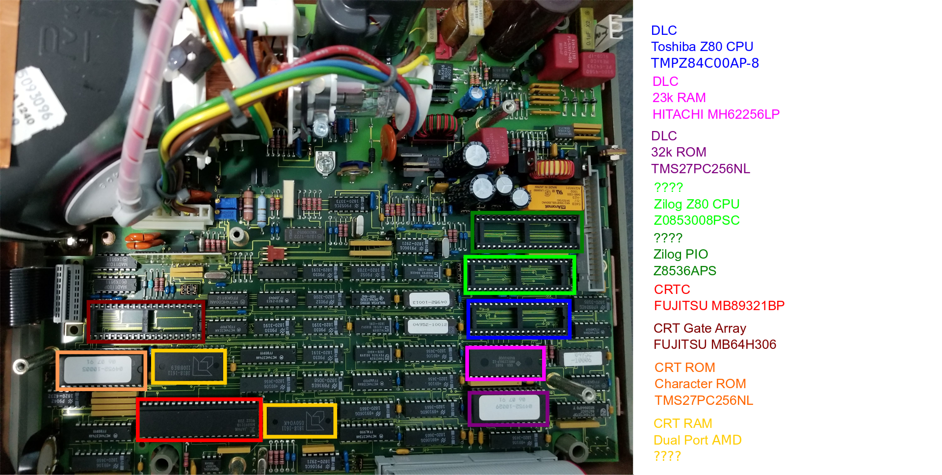
Main Board Breakdown
12/31/2018 at 22:35 • 0 comments![]()
On the bottom left we have all the CRT controls. The two AMD chips are presumably dual port RAM chips as the previous several 4951's all used this to eliminate any bus timing issues.
The DLC is not listed on the 4951C schematics but it has its on 32k RAM & ROM.
The Green chips are a z80 and PIO that connect to the pod pin-header. When removed the system still passes the self test so that weird. Apparently the "Remote" processor is the 8051 on the memory board. Maybe this is the capture streaming processor only and just relays data.
-
GAL's Unfortunately
12/30/2018 at 00:21 • 0 commentsI have the repair manual for the 4951C which was the early model of the 4952A. The unit is effectively the same but the main board and memory board are totally different.
The one thing that is exactly the same is the floppy controller board. From this schematic I have verified that all the "double wave" logo'ed ic's are in fact National Semi GAL's. This means the bus decoding is inside the black box and requires probing to identify. That is no simple task.
The floppy board did give me the complete riser pinout though, so from that I at least know the interface. If I can isolate things to similar components I may be able to find a starting point.
-
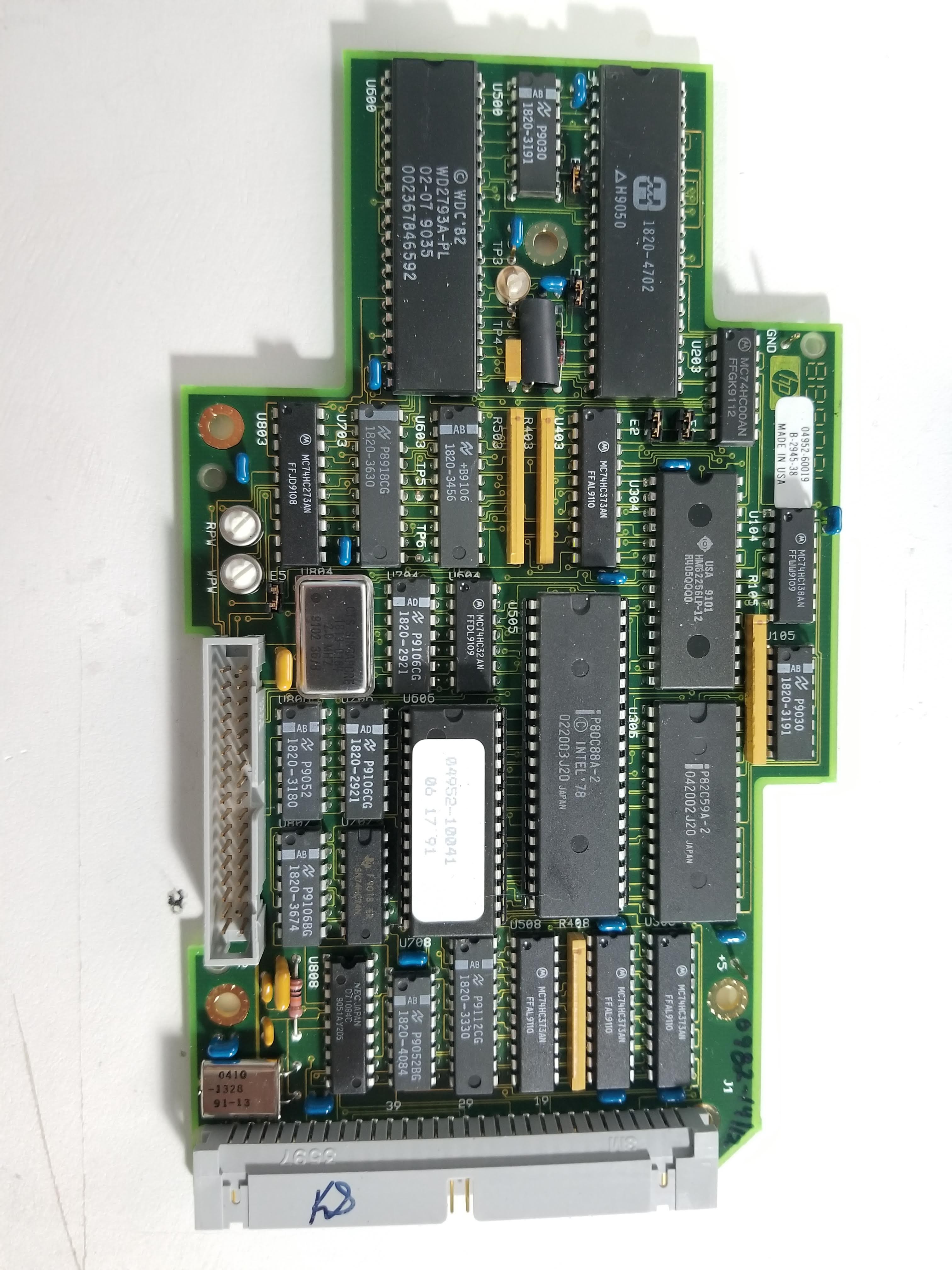
Floppy Controller
12/29/2018 at 06:53 • 0 commentsThis is a dense little board. It has as the standard bits a floppy controller needs like the WD2793A which is the goto chip. The very interesting part is that this board has RAM, ROM aaaaaand a full 8088 x86 CPU.
The 8088 is another one of those weird 32 bit processors with only an 8 bit bus. Makes me wonder if this board all by itself can be turned into an SBC. Heck, with more ram maybe it could run DOS all by itself?
![]()
-
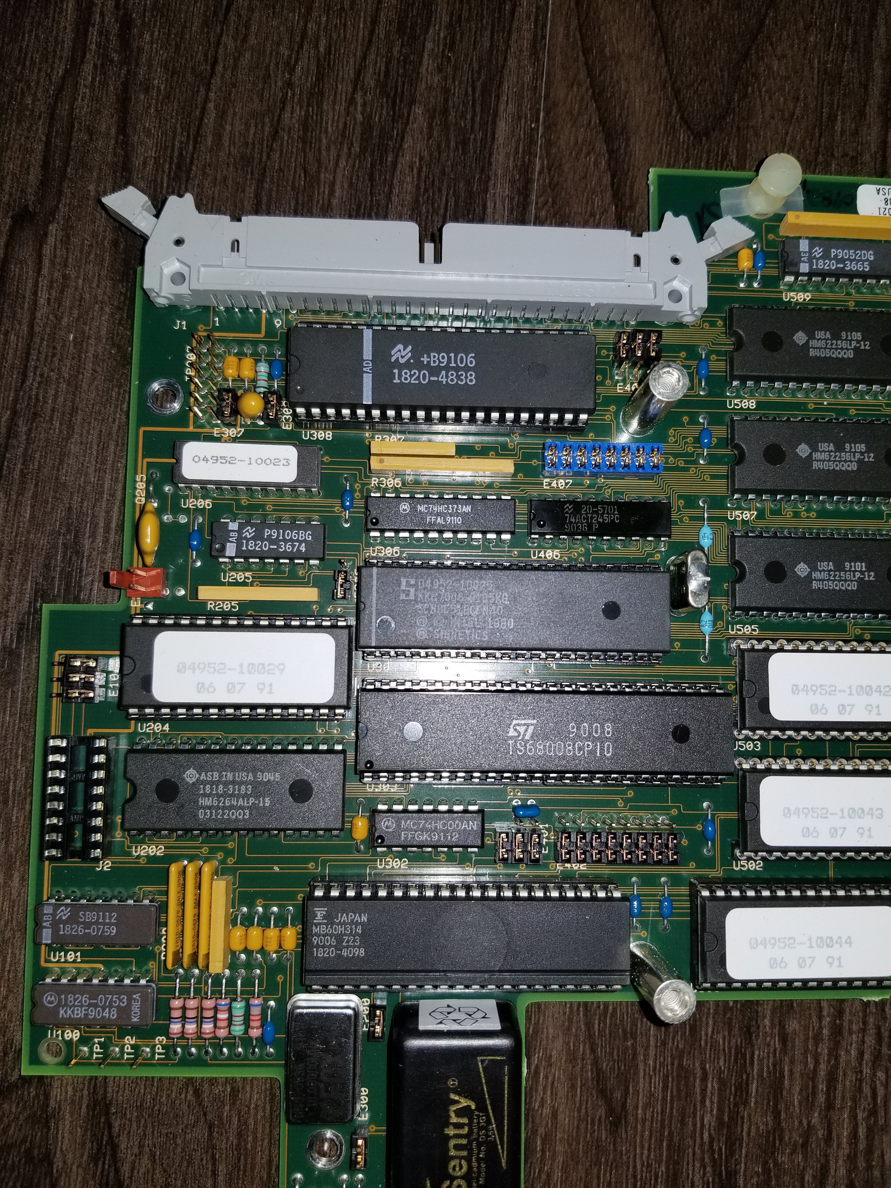
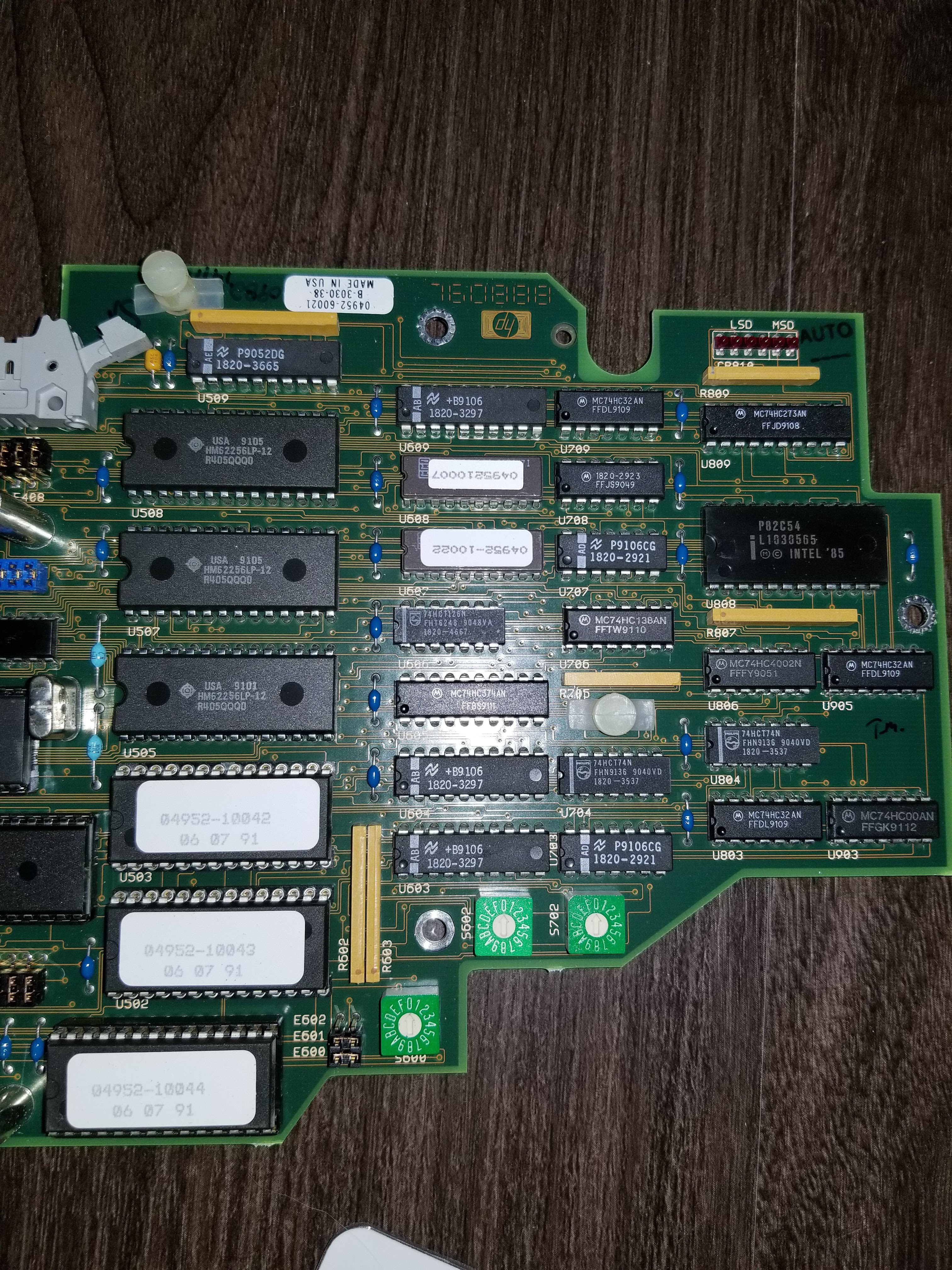
Memory Board?
12/29/2018 at 06:44 • 0 commentsBus connection ribbon cable leads to TWO strange processors. One TS68008 which is a weird 32bit CPU with only an 8 bit interface. The second is an Intel 8051 CPU. The random 32 bit processor is strange.
I have to wonder if this is not actually the "brain" of the machine and the two z80's on the main board are just for IO and presenting data to the video hardware maybe?
![]()
Bunch of SRAM and some card ID selector switches. Also some random LSB/MSB LED's.
![]()
HP 4952A turned general purpose CP/M machine
Attempting to reverse engineer an HP 4952A into a general purpose z80 computer capable of running CP/M.