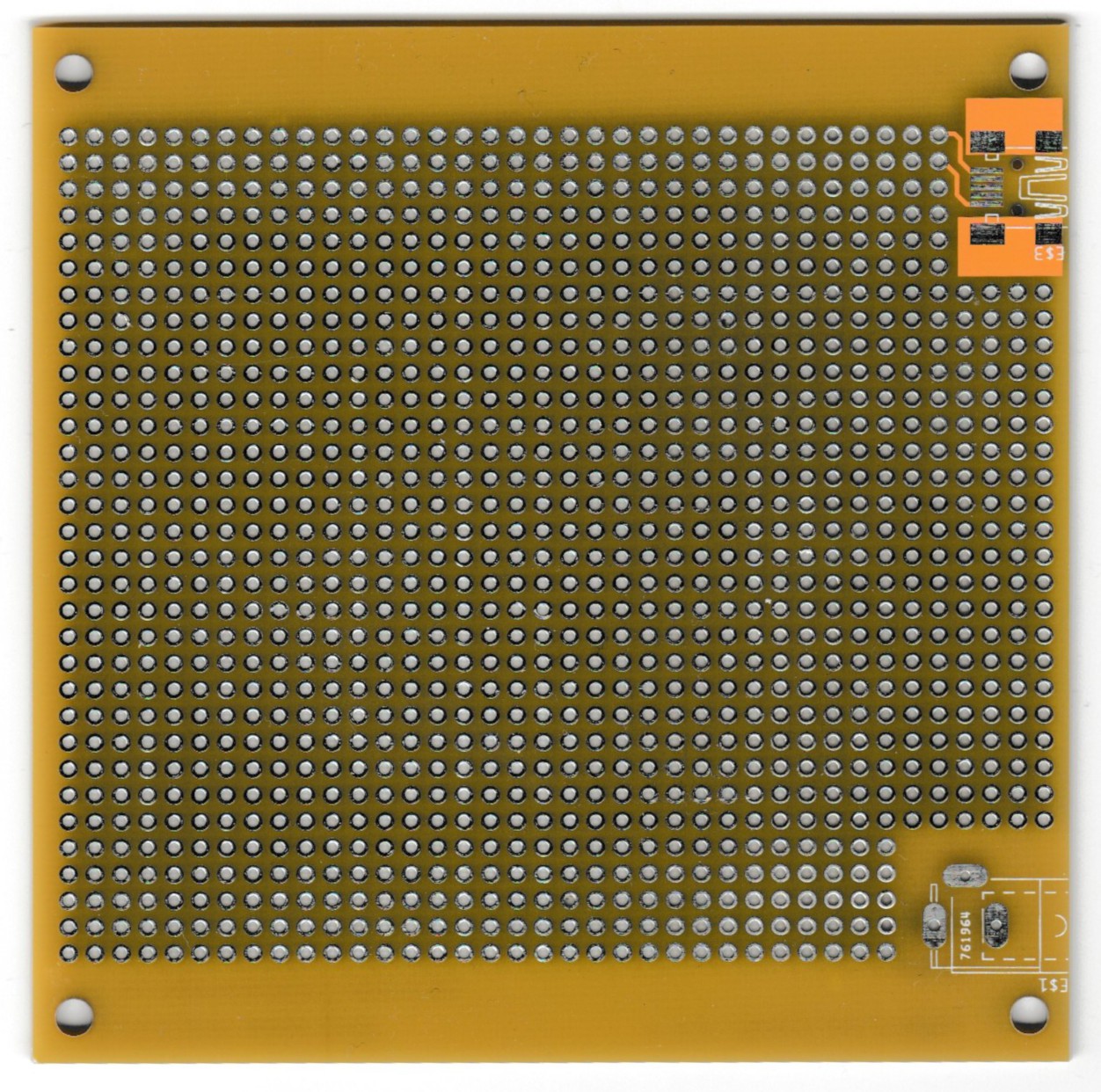
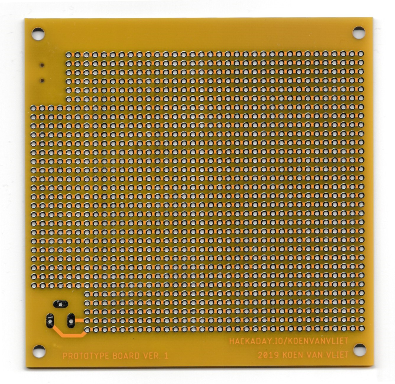
Some pictures of the bare prototype boards I made on my flatbed scanner


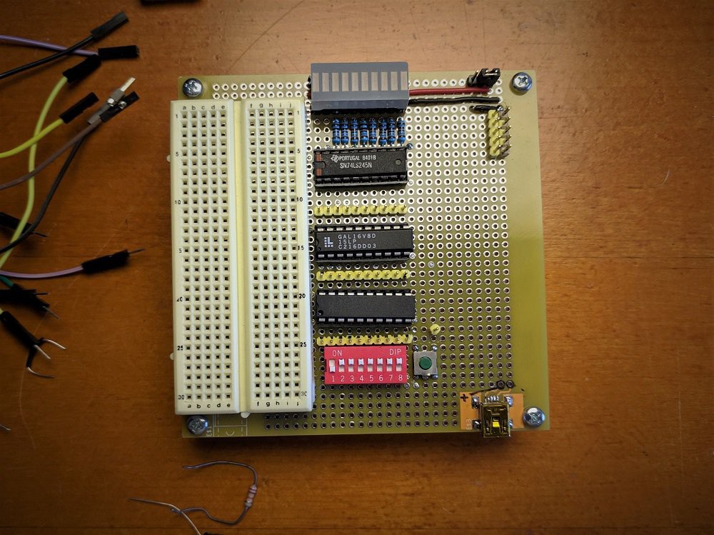
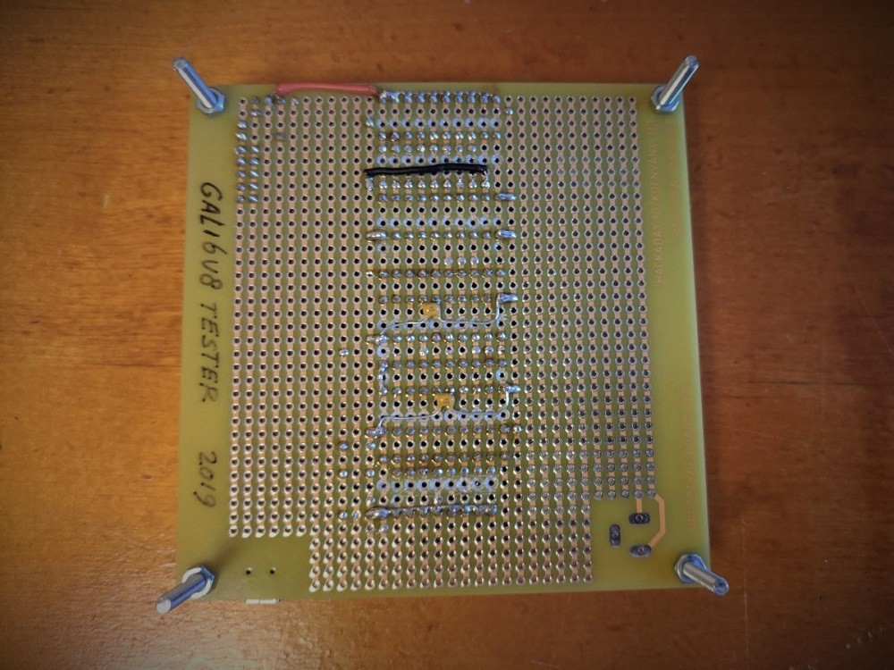
I found that the prototype board 1 is very suitable for logic ICs. The old board layout techniques of vertical lanes on the bottom and horizontal on the top layer works really well on stripboard. Here is an example with (bottom to top) some switches, two GAL16v8 programmable logic devices, a line driver and an LED array.
Edit: The breadboard is not part of the board. I placed it on the PCB with double-sided tape for some quick prototyping.


Evaluation
Overall
- Very nice quality stripboard with accurately drilled trough-plated holes.
- Solder flows nicely. Thermal mass not too high.
- Solder mask prevents solder blobs. This is usually an issue on traditional bare stripboard.
- Traces are easily cut with a knife or drill bit.
- Trough plated holes can be soldered on top side as well. Very useful for the occasional SMD component. (the SMD button shown above)
- The PCB is warped a bit, because there is more copper on the bottom side of the board. Less than 1 mm across the 100 mm PCB.
Connectors
- The USB connector is easy to solder due to the indexing holes.
- The DC barrel jack connector footprint was incorrect, so the slots were not milled out.
Possible new features
- I feel like the USB data pins should also be broken out.
- Perhaps it would be nice to have an USB microcontroller circuit directly on the prototype PCB. This could be used for USB to serial (or any other protocol) or even HID device, who knows.
Solder pads are smaller than other prototype boards I have used, but this did not bother me while building this circuit. It actually reduces the risk of solder bridges. That said, it's still easy enough to create solder bridges to join two traces together.
Final thoughts
Very nice quality and usable prototype boards. I will address the issues in v1.1 and possibly add some new features.
 Koen van Vliet
Discussions
Become a Hackaday.io Member
Create an account to leave a comment. Already have an account? Log In.