 Corey Benn
Display Layout (from behind, left to right)

       A12345
       B12345
       C12345
       D12345
       E12345
       F12345
(Z123) G12345


Connection Blocks (mapping)
B1 F1 A2 G2 | E3 B4 F4 A5
A1 G1 D1 F2 | F3 A4 E4 B5
Z3 C1 E1 E2 | G3 D3 D4 C5
Z2 Z1 B2 D2 | C3 C4 E5 G5
Z1 Z1 C2 A3 | B3 G4 D5 F5
I traced the connection block pins to the corresponding display dots. There are 3 traces which interact with the reed switch, these are to the far left when looking at the back of the display, which I've labeled as "Z".
Directly applying voltage to a single dot with a standard 5 volt USB power source, a single dot can flip. Reversing the polarity will cause the dot to flip back to the other state.

 kmatch98
 zanzeoo
 Dave's Dev Lab
 w_k_fay
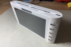
Pretty beat up, but still decent looking. Hope you can bring it back to life - love flip dots!