Observations to explain:
* applying large negative voltage to gate => lowering threshold
* applying large positive voltage to gate => lowering threshold
First, a painting of mosfet with no voltages applied.
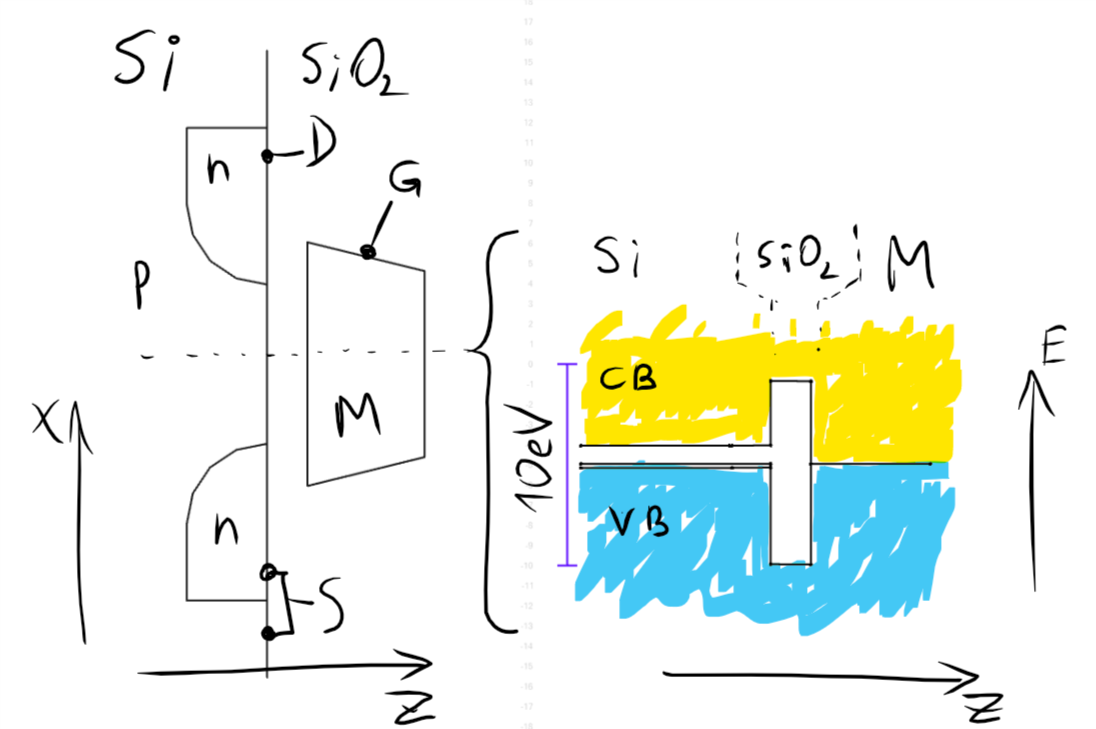 On the left, cross-section of the device is shown (n-channel MOSFET). Dashed line is a cross section for which band diagram is drawn.
On the right, I painted a band diagram along a section line. I have taken band positions from this page:
http://www.nextnano.com/nextnano3/tutorial/1Dtutorial_pSi_SiO2_polySi.htm
Yellow fill is empty electron states. Blue fill is filled electron states. White area is forbidden zone (bandgap). Horizontal line in the middle is Fermi energy, in this case equal for both sides, as there is no voltage applied.
There might be built-in field because of difference in work functions between base material and gate material, but I just assume they are equal, for simplicity.
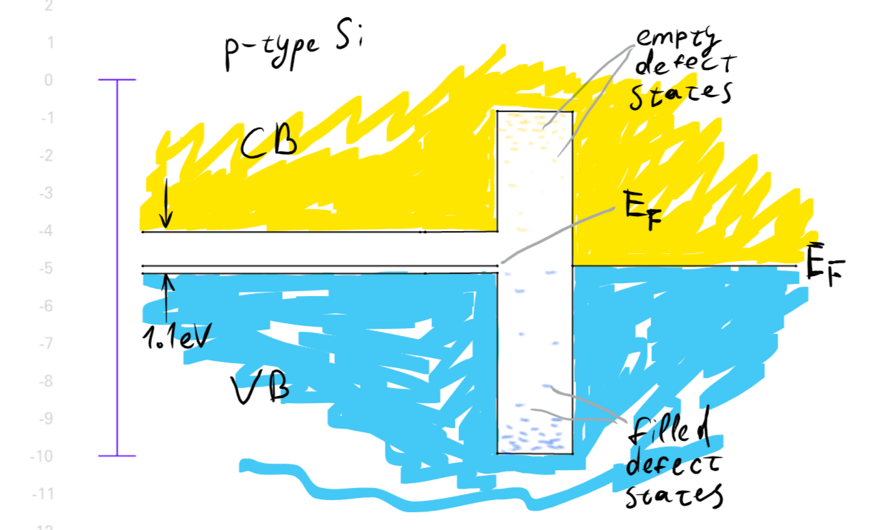
Closeup of the band diagram. Defect states in SiO2 are shown.
Now, here comes the diagram for transistor under torture.
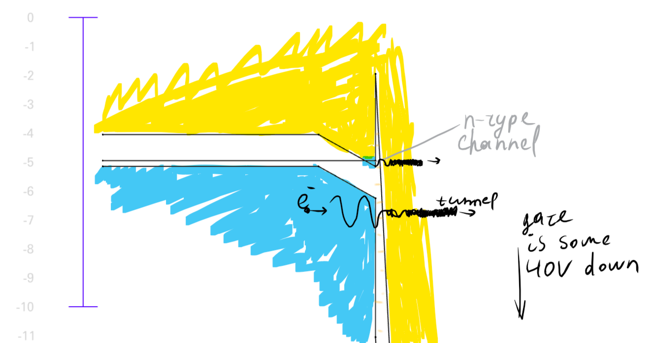
... up at the Si side... and ... down at the gate side...
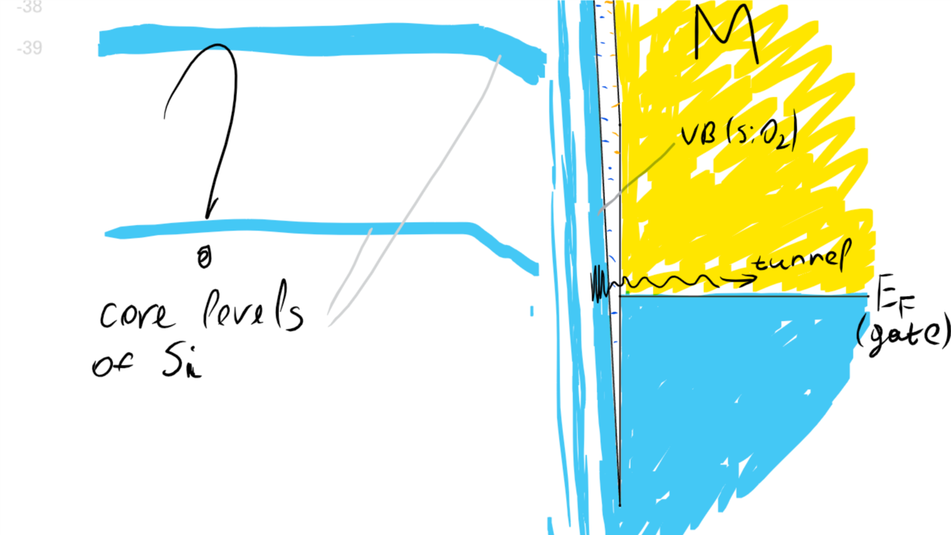
That was for positive voltage (40 V) applied to gate.
Now, for negative:
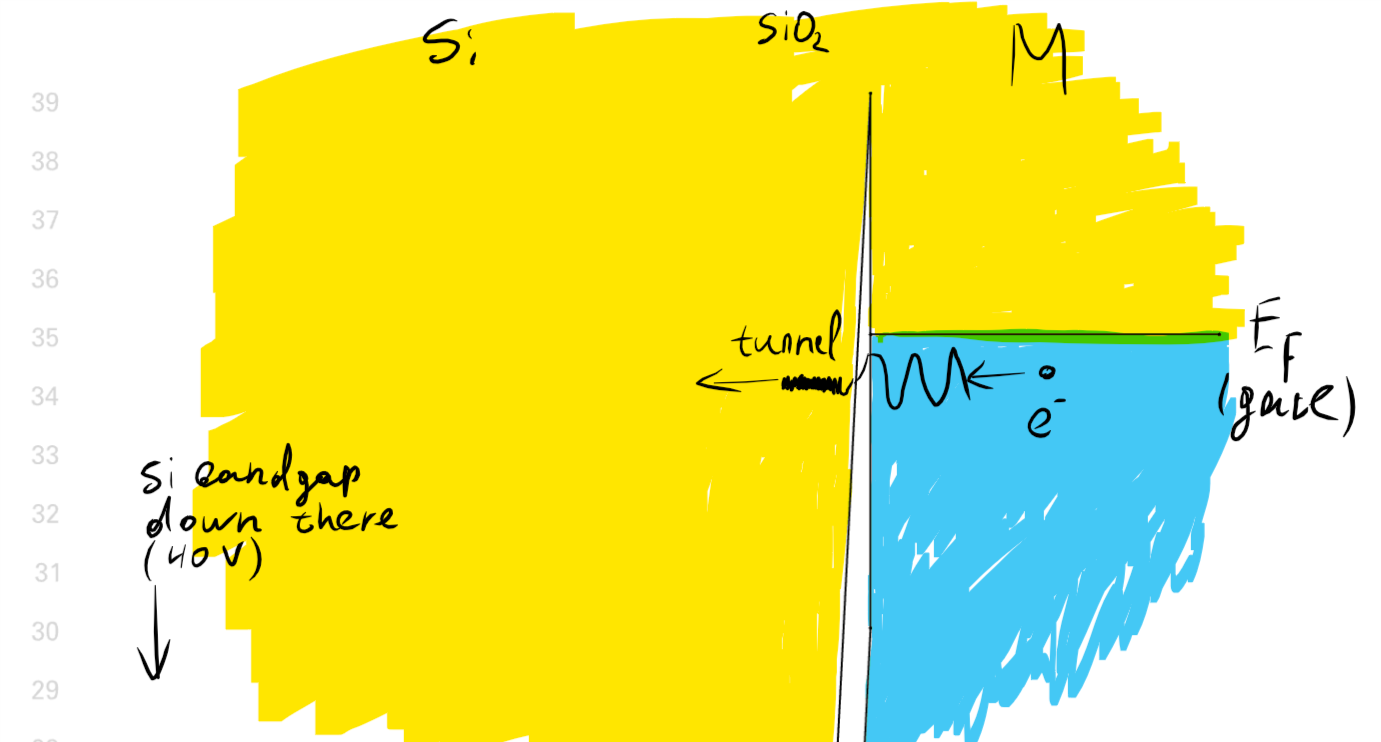
... up at the gate side... and ... down at Si side....
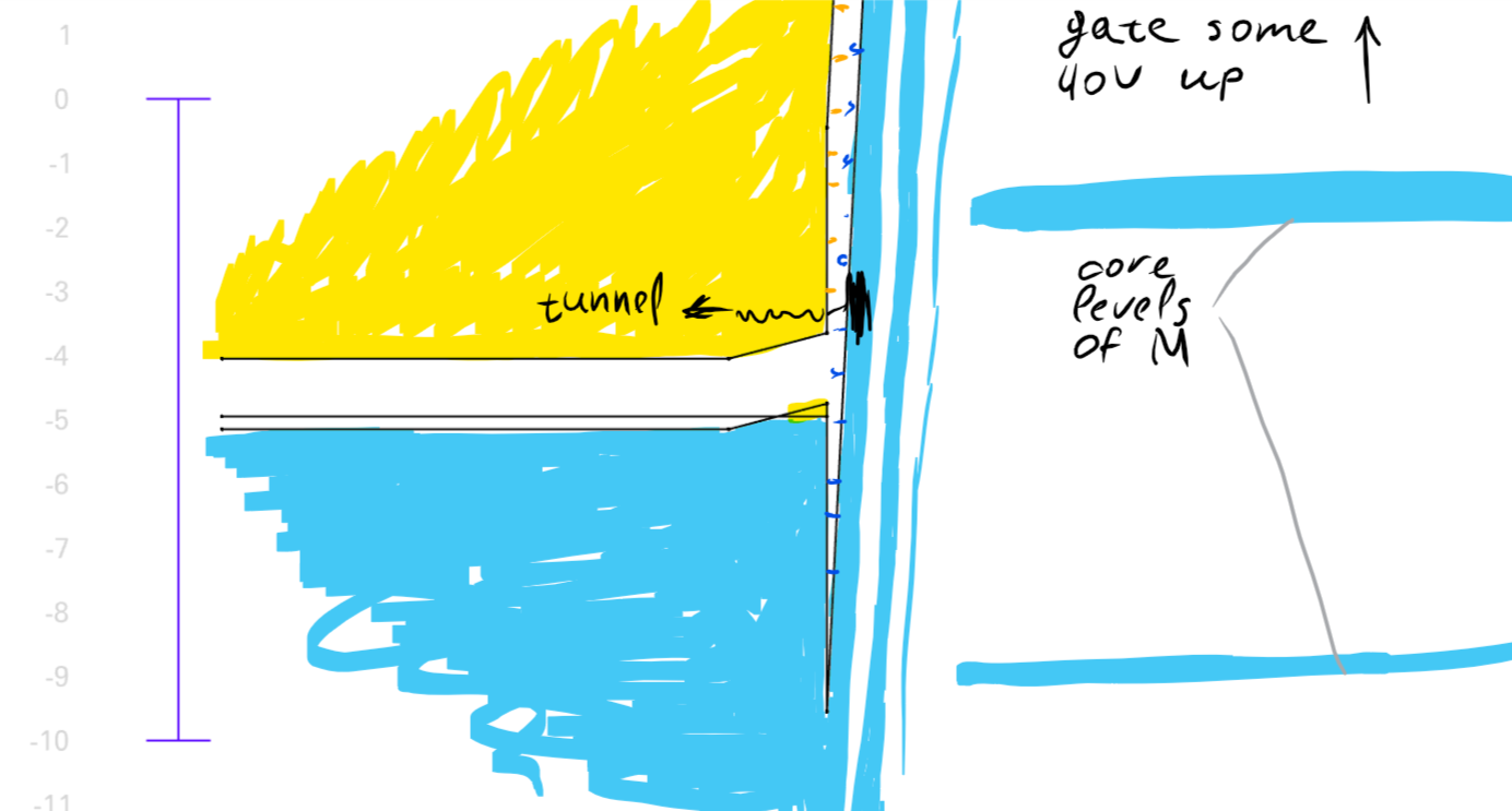
These were drawn with no explanation of the mechanism. These pictures are pretty general, and I hope there isn't much that I could get terribly wrong here.
... more to come...
 DeepSOIC
Discussions
Become a Hackaday.io Member
Create an account to leave a comment. Already have an account? Log In.