 Alastair Hewitt
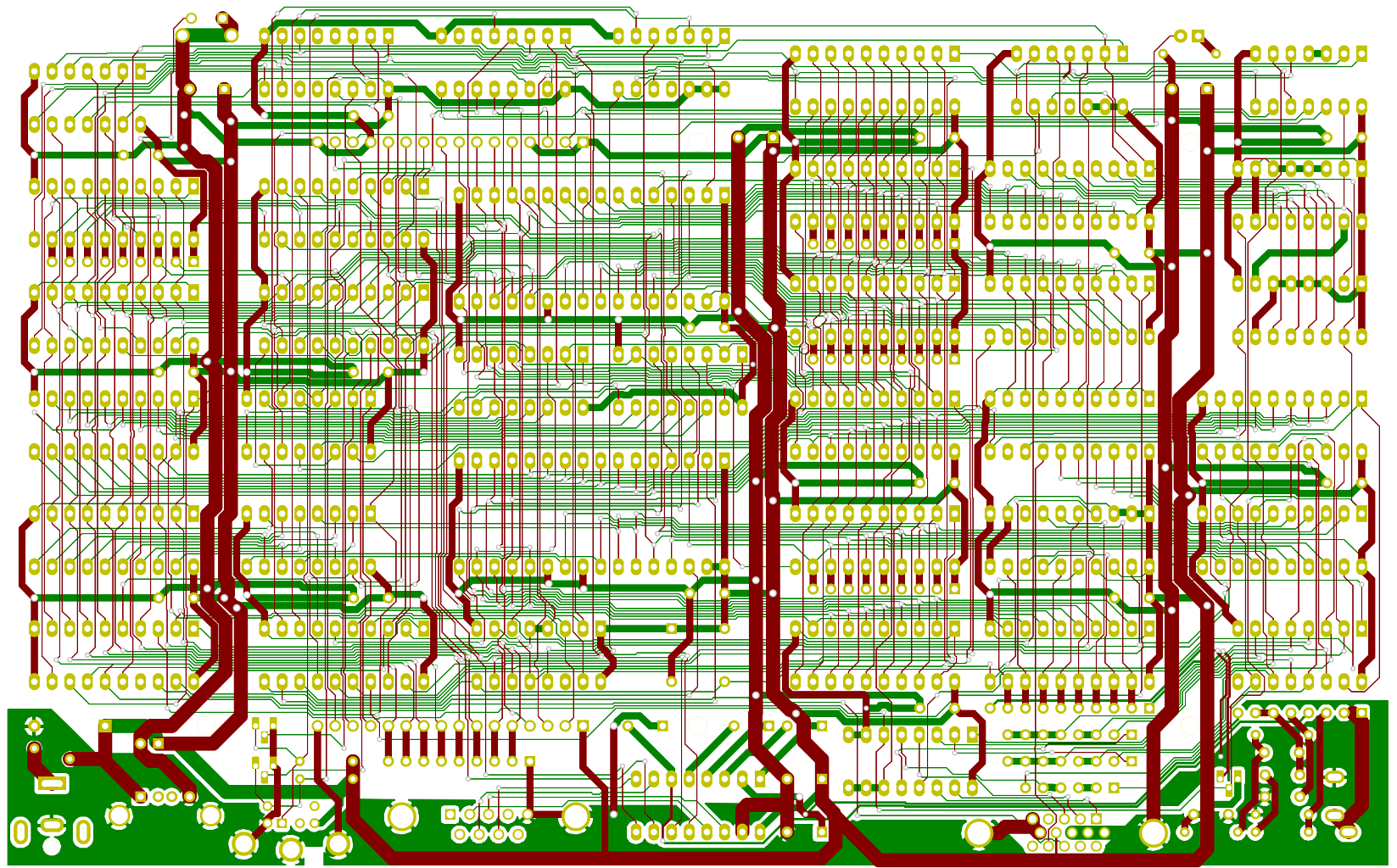
Hot off the press... Routing was just completed using 8 mil traces with 7 mil spacing. This was 100% hand routed and took about 30 hours. The original attempt using 10 mil traces with 8 mil spacing failed after about 24 hours of work.
The ability to route two traces between the DIP pads was the only way to complete routing at this density (40 chips on 8" x 5" double-sided board). Extra space was also added around the ROM to allow a ZIF socket to be installed.
Update: DRC checks pass and initial visual inspection done. The power barrel jack needs fixing and possible additional mods after further review. If everything checks then it will get shipped for fabrication tomorrow.
Discussions
Become a Hackaday.io Member
Create an account to leave a comment. Already have an account? Log In.
lovely work!
Are you sure? yes | no
That's impressive. Layout cost me 10 weeks.
Are you sure? yes | no
Technically I've been working on this for 22 weeks :) I spent a lot of time playing with the layout but didn't want to do any routing until I'd finished modifying the design and tested the final version on the bread board. Then it took about a week since the first attempt failed.
So I had a pretty good understanding of how to route things by the time I got to this point and was able to go from component layout to routed board in 30 hours.
Are you sure? yes | no
>This was 100% hand routed and took about 30 hours.
Respect! 👍
Are you sure? yes | no
That's impressive! Congratulations!
Are you sure? yes | no