 Alastair Hewitt
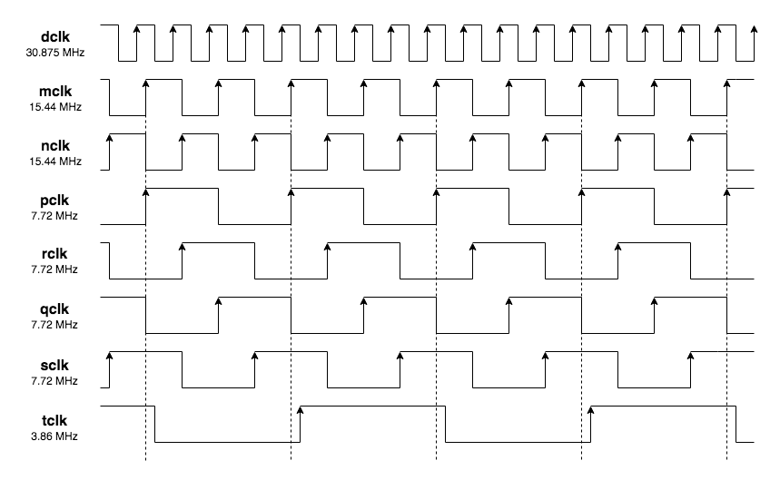
The clock circuit consists of a Pierce Oscillator running at 30.875 MHz and two Johnson Ring Counters. The first ring counter (mclk/nclk) consists of a single flip-flop to divide the 30.875 MHz dot clock (dclk) down by a factor of 2. The second (pclk/qclk) consists of two flip-flops to divide the dot clock down by a factor of 4. The last stage of this counter is duplicated to provide an additional set of identical clocks.
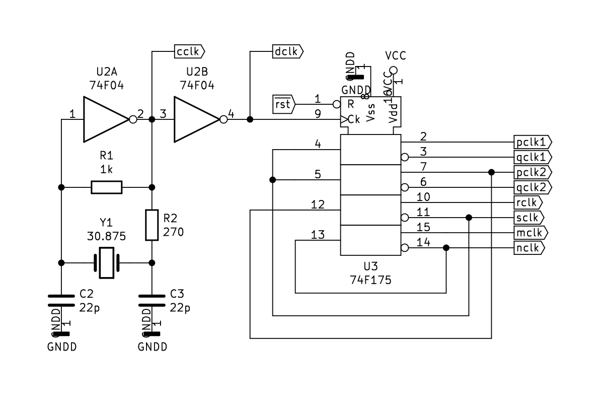
Some considerations in this design:
- A single clock source is used to derive all the other clocks, rather than feeding the clock of one flip-flop with the output on another. This keeps all the clock edges aligned.
- The rising edges of the mclk and the pclk/qclk must to be synchronized. This requires the flip-flops to be reset on initialization or after power fluctuation.
- The pclk and qclk control complementary bus contexts. The complementary outputs of a single flip-flop keeps these perfectly symmetrical and avoids bus contention, especially when held in reset.
- The pclk and qclk are both used 11 times throughout the circuit and this exceeds the maximum TTL fanout for a single output. Two sets of these clocks are generated and divided evenly so no one clock output serves more than 6 inputs.
The following shows the clocks generated by the circuit above. The tclk is also included for reference, but not shown in the circuit.
Discussions
Become a Hackaday.io Member
Create an account to leave a comment. Already have an account? Log In.