Alastair Hewitt
-
Rev. 6
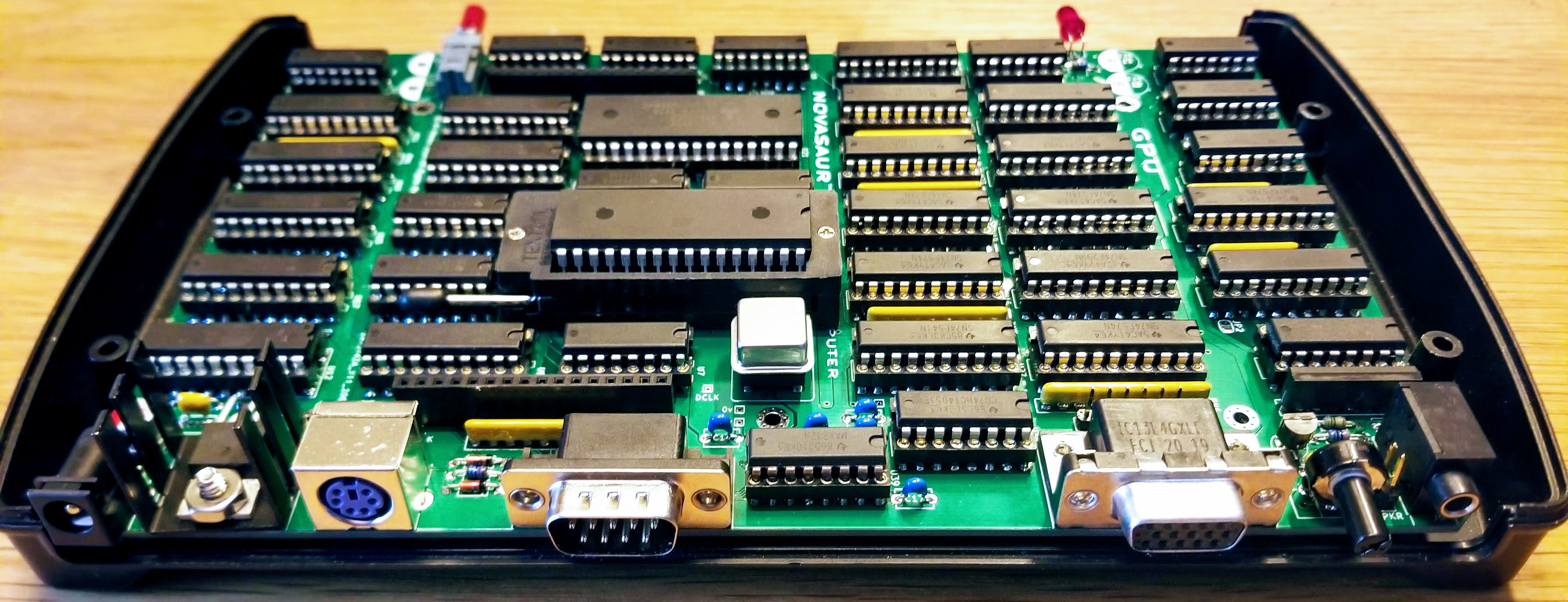
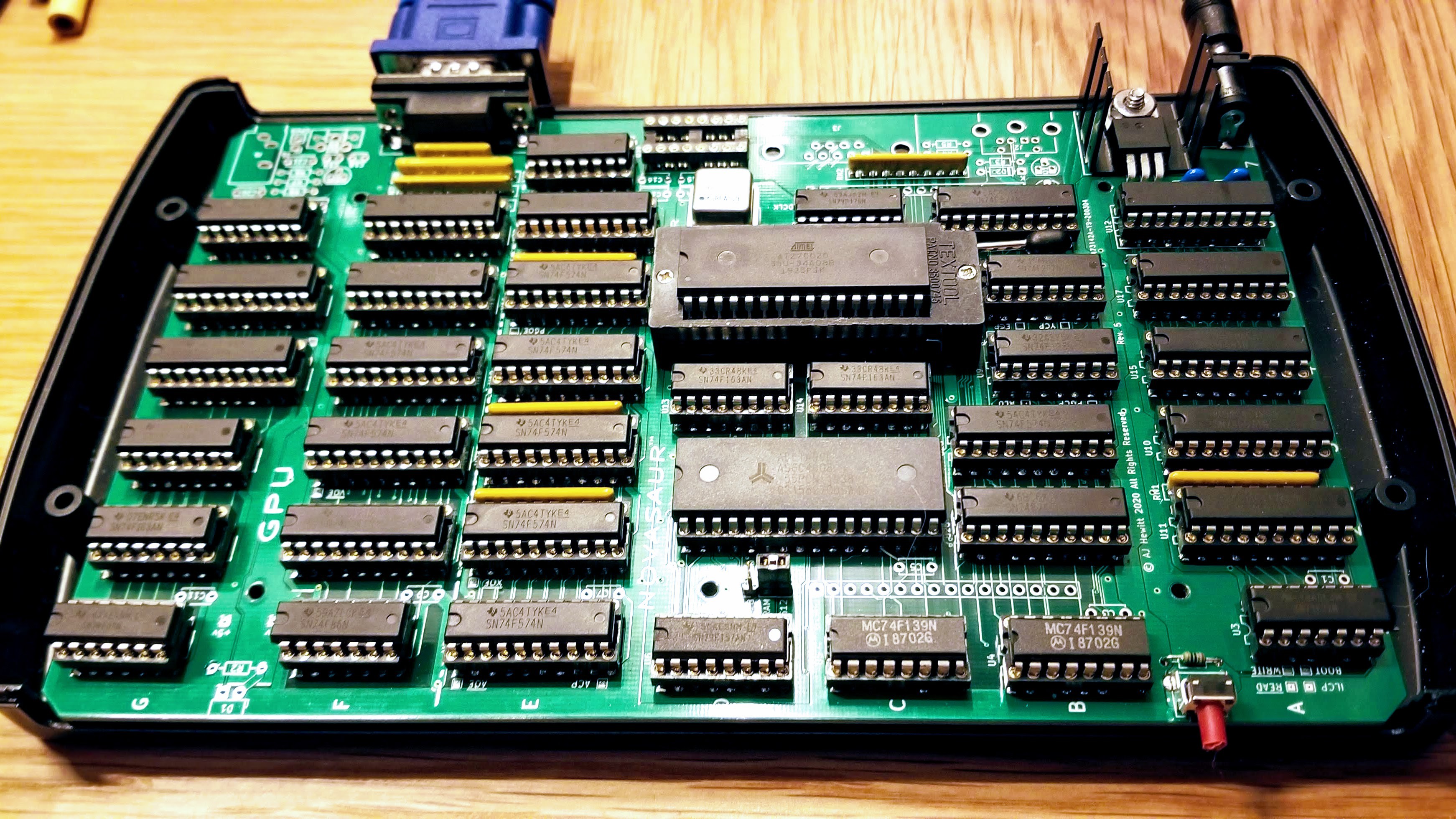
08/13/2020 at 19:44 • 0 commentsThe hardware abstraction layer development has taken an entire year and is finally nearing completion (final details in an upcoming log). In the meantime there were some minor updates to the hardware, some of which were discussed in the last log. This resulted in the rev. 6 board shown below:
![]()
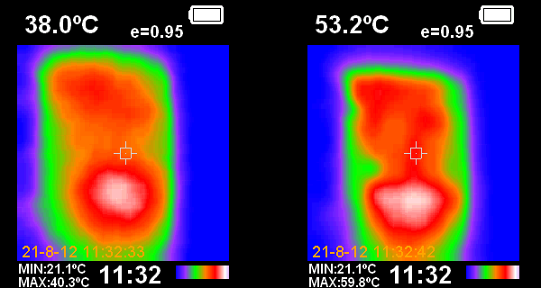
It was time to do a more detailed thermal analysis to make sure this hungry beast will not overheat. The F-series TTL chips consume about 5mW per gate and the 1,425 gates making up the Novasaur dissipate close to 7.5W. The regulator also dissipates up to 1.5W for a total power consumption of 9W.
The plan is to have a sealed enclosure, so no ventilation holes. The components are cooled by radiating heat that is absorbed by the case. The case then radiates this heat to the environment until it reaches a thermal equilibrium. At this point the temperature is stable and the best way to measure this is via a thermal imaging camera.
A budget camera was obtained and some initial measurements made. The picture on the left is the external case temperature after running for about an hour at 21C ambient. The picture on the right is with the cover removed showing the circuit board.
![]()
There is a hot spot reading around 41.5C from the outside of the case and 62.5C from the inside. This area is centered around the B, X, and Y registers. The B register is the pipeline between the data and program address space and clocked at 16.5MHz. Both the X and Y register have pull-up resistors and are cycled at a similar rate. Together these three chips represent the highest heat density on the board.
![]()
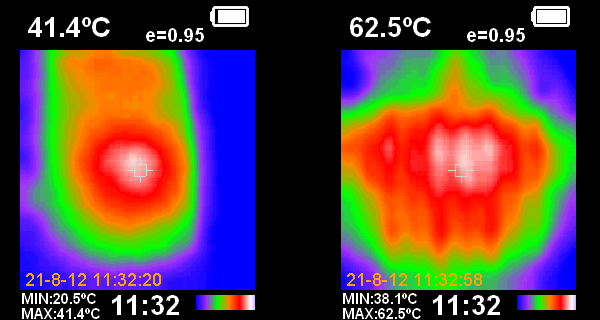
There is a second hot spot over the regulator shown in the left picture below (the H shape towards the bottom is the heatsink). The spot above that is the PAL, which also runs quite hot. It's interesting to note that the regulator is slightly cooler at 60C than the hottest chips.
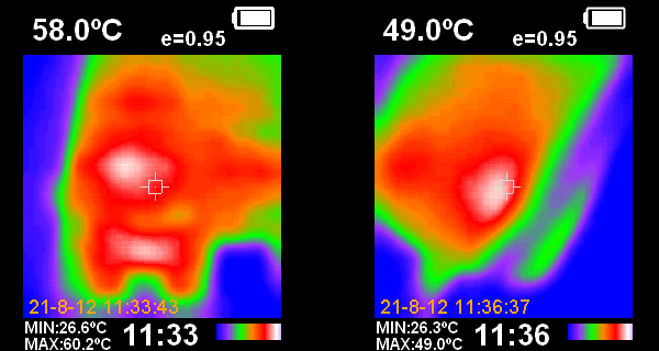
For comparison the picture on the right shows a hot spot on the 6V power adapter case. This had a temperature of 49C, which was several degrees above the Novasaur case.
![]()
Note: These were just some initial pictures and more accurate and detailed images are planned. The emissivity was the default 0.95, but it is probably more accurate at around 0.90.
-
Video DAC
07/04/2020 at 04:30 • 0 commentsIt's been a month since the last log, so I thought I'd check in. Other priorities have taken over a bit so I'll cover one minor change that was made to the PCB design. This started with an examination of the Video DAC placement to see if the current VGA connector could be changed.
The original PCB design used a low-profile VGA connector due to space constraints. Not only did this cost 2.5x as much, but the only distributor was out of stock for 4 months. This is a big risk for a kit version, so the change was made to fit the more common larger-sized connector.
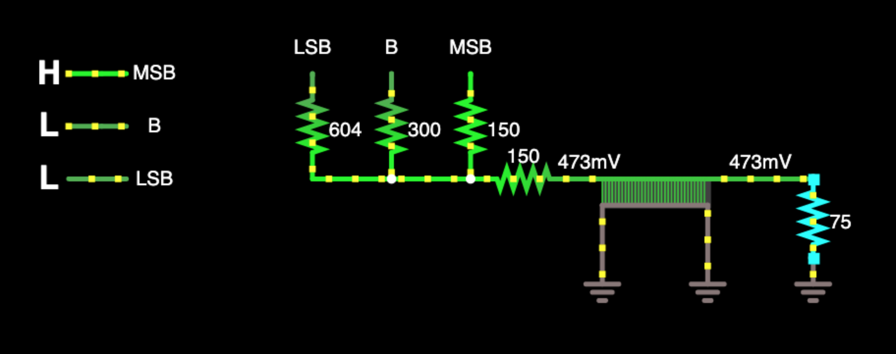
The original video DAC had to be moved and it was a good chance to re-examine the design. Calculating the resistor values for the DAC gets quite complicated, so in the end it was just easier to simulate the circuit and play with it.
![]()
The circuit above shows the channels of a 3-bit DAC with resistors used to divide down each bit by a factor of two. The analog switch has a fairly large on resistance shown as a 150 ohm load in series with a transmission line to the monitor load of 75 ohms. The state shown in the circuit is with the most-significant bit high and the other two bits low. Low does not mean off, these other outputs are sinking current in their low state.
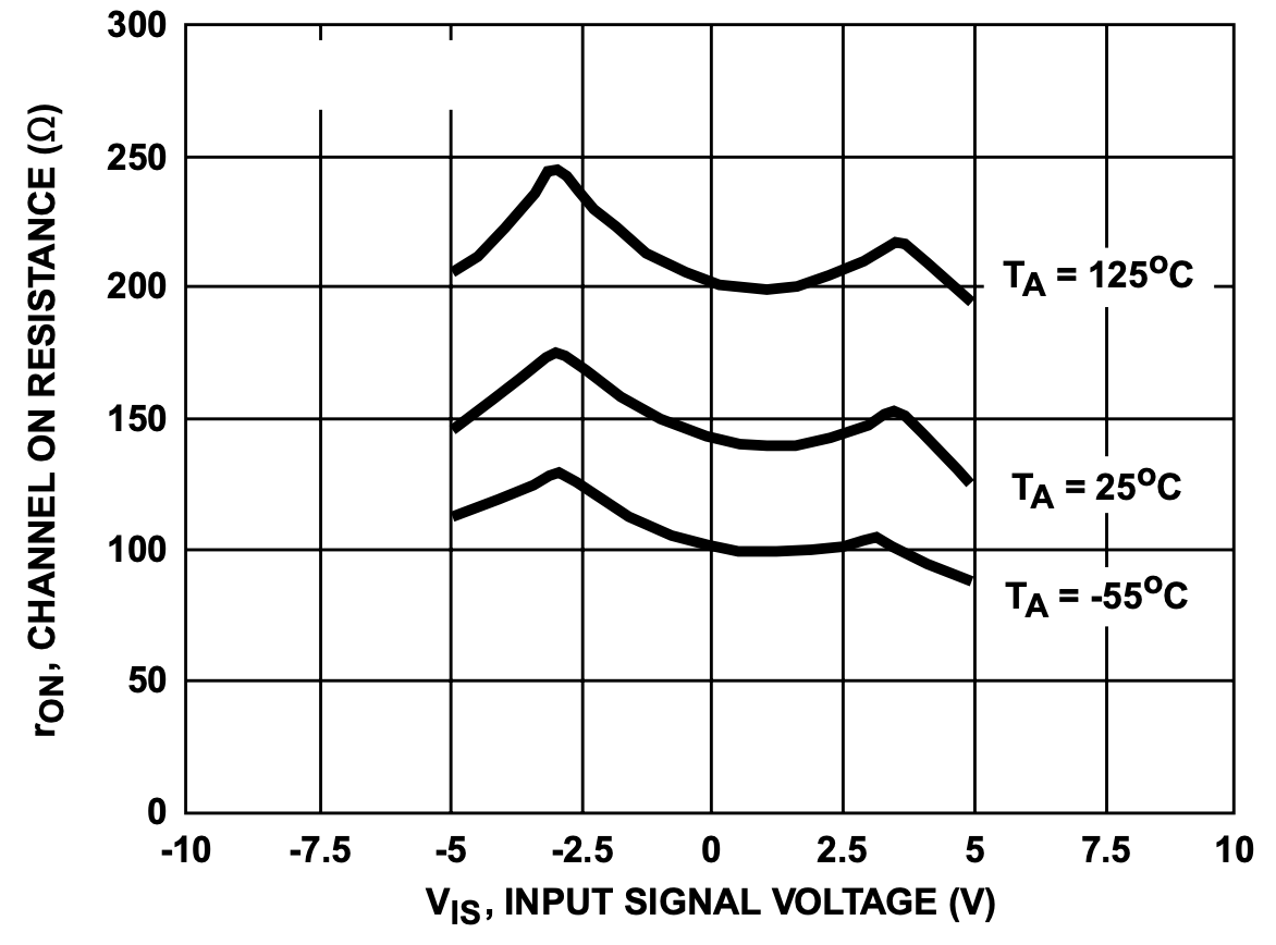
The circuit assumes a high voltage of 3.2V and a low voltage of 0.3V. The 150 ohm resistance of the switch comes from the data sheet for the CD4053 being driven with a VCC-VEE voltage of 10V (the negative VEE is supplied by the RS232 driver).
![]()
There are a couple of drawbacks with this simple DAC design. Since the low voltage is never 0V then there is no completely black color, only very dark gray. Since the blue channel is only two bits it varies from 0-3, where the red and green vary from 0-7. Seven doesn't divide into three, so there are no actual gray colors.
The on resistance of the analog switch also changes as the chip warms up. The resistance could change by up to 20% from an initial 150 ohms at 25C to 180 ohms at 60C. The following color palettes were generated from the simulation to show the difference between 150, 165, and 180 ohms:
![]()
![]()
![]()
The difference is fairly subtle, so the temperature change shouldn't be too noticeable. For comparison, this would be the ideal palette with the correct DAC voltages:
![]()
There are no resistors used with the 8-color text "DAC". Each bit is passed directly to the analog switch, which when combined with the monitor load divides the voltage by 3.2. This gives a value of about 0.1V for low and 1V for high. The text mode will always saturate the color, but also never be completely black.
-
Interrupts
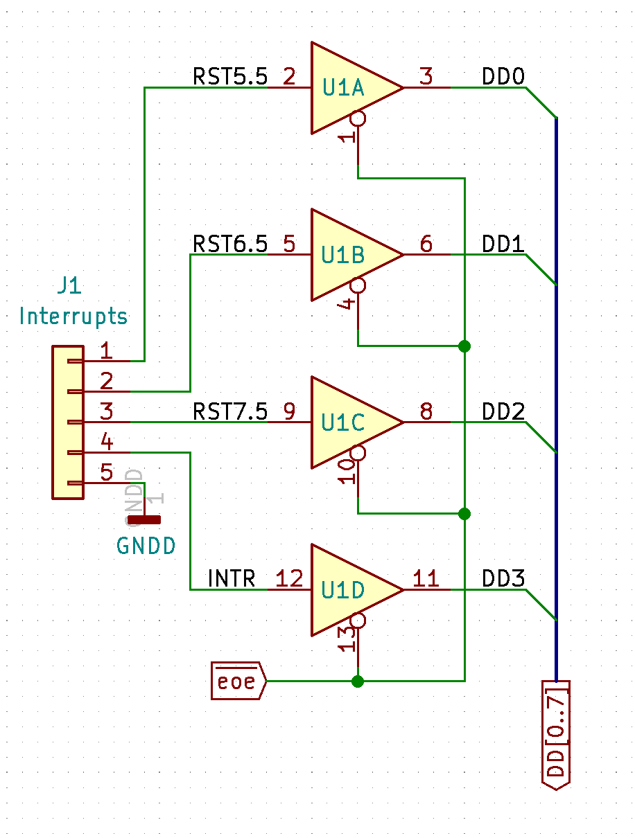
06/04/2020 at 21:06 • 0 commentsThe 8080 development has been extended to support most of the additional features found in the 8085. This includes four of the five hardware interrupts. This is possible because the lower nibble of the Ei register is available via the expansion header. A buffer controlled by the ~EOE signal can be used to read the interrupts as shown.
![]()
Software Interrupt
The 8080 provides eight software interrupts via the RST 0 through RST 7 instructions. These will jump to the vector n * 8, where n is the number after the RST. The virtual CPU executes these interrupts using the code rst.nsa followed by restart.nsa. The first single-cycle RST instruction will increment the program counter, load the temp register with the lower 8-bits of the reset vector, and then rewrite the instruction to RESTART. The two-cycle restart instruction will push the program counter on to the stack, clear the upper program counter byte, and then copy the reset vector from the temp register to the lower program counter byte. The instruction at the new program counter address is then fetched and the instruction cache updated.
The original Micro-Soft Altair BASIC 3.2 used the RST instructions to call common subroutines. This was primarily to reduce program size since this is a single byte instruction rather than the typical 3-byte CALL which must specify the 16-bit subroutine address.
Hardware Interrupt
The 8080 provides one hardware interrupt via the INTR input. This is enabled via the EI instruction and disabled via the DI instruction. The 8085 adds an additional four interrupts: RST5.5, RST6.5, RST7.5, and TRAP. The TRAP interrupt is non-maskable and used to initiate things like a power shutdown. A client of the hardware abstraction layer (HAL) would not have this level of privilege, so this interrupt is not implemented.
The first three interrupts act like the RST instructions, except they are offset by an additional 4 bytes, so RST5.5 is the vector 5.5 * 8. The INTR interrupt will read the value of the I0 register and use this as a vector into the zero page. This could be set according to some external state to control the program flow.
An interrupt can only take effect during the fetch cycle, but the current fetch cycle does not have enough cycles to handle the interrupt mask. The solution is to treat the interrupts as another feature of the HAL and control them via the feature flag IMODE.
The IMODE flag is set at the beginning of the virtual process cycle if the interrupts are enabled. The fetch cycle checks the IMODE flag and if set will fork from the standard fetch operation. In this case the IMODE flag is reset and the INTR1 instruction is written to the instruction cache. This instruction is executed in the next machine cycle and applies a mask to the Ei register to see if any of the unmasked interrupts are set. If an interrupt is set then the associated vector is written to the temp register and the RESTART instruction is rewritten to the cache. If the interrupts are clear then the fetch cycle is completed and next instruction written to the cache.
This way the interrupts are checked once per virtual process cycle at the expense of one virtual machine cycle. Most applications would not use the interrupts and the IMODE flag would not be set. In this case there would be no impact on the virtual CPU performance.
Mask
The SIM instruction sets an interrupt mask based on the contents of the accumulator. The lower 3 bits (0-2) will mask the RST5.5, RST6.5, and RST7.5 interrupts respectively (when set high). Bit 3 represents the interrupt enable state, so will have the same effect as calling DI if set low and EI if set high. There is no additional mask for INTR, so it is always active when the interrupts are enabled.
The RIM instruction reads the current interrupt mask and stores it in the lower nibble of the accumulator. Meanwhile the current value of the interrupts is stored in the upper nibble. This provides access to the state of the interrupt lines without having to enable the interrupts.
There is a hidden feature where the upper nibble of the accumulator will mask the rest of the Ei register as if it were more interrupt lines. This is where the serial inputs are located and in effect these lines could be used to trigger additional interrupts. Typically the upper nibble of the mask would be set to 0000, but setting any of the bits to 1 will unmask that line and cause an interrupt when the respective serial input is high. Note: this mask state is the opposite of the standard mask bit. These interrupts map to RST1.5, RST2.5, RST3.5, and RST4.5.
The interrupts are prioritized according to the number, where RST7.5 is the highest. If more than one interrupt line is set, then the highest priority will take effect. The INTR interrupt is the lowest priority, coming after RST1.5.
Halt
It's also worth noting the operation of the HLT instruction here. This effectively stops the CPU and waits until there's an interrupt before continuing execution. The halt instruction will increment the program counter, but then rewrite the INTR2 instruction to the cache. This is almost identical to INTR1 described above but does not fetch the next instruction if the interrupts are clear. In this case the INTR2 instruction is returned and the cycle repeats, leaving the CPU in an infinite loop until an interrupt is detected.
This way the interrupts are checked once per virtual machine cycle in the halted state. Execution will resume from the instruction after the HLT when the interrupt service routine ends with the RET instruction.
-
Serial IO and the vUART
05/24/2020 at 03:34 • 0 commentsThere are two serial ports and only their physical interfaces are implemented in hardware. This means everything above layer one has to handled by software in realtime. There's no shift registers to hand off parallel data, only single bits in the Ei and Eo registers for the data, control, and clock signals.
![]()
Modes
Along with the video timing and wavetable synthesizer, the hardware abstraction layer also implements a virtual UART (vUART). This is also an optional feature and is controlled in a similar way to the audio using a serial mode.
Mode Interface VMCs CPU Eo bits -1 None 0 100% xxx10xxx 0 PS/2 0.1 99% xxx11xxx 1 RS-232 1.9 87% xxx0Dxxx Note that the vUART only handles one type of interface at a time. This is possible because both interfaces implement hardware flow control: The RS-232 uses RTS/CTS flow control and the PS/2 interface can be inhibited by grounded the clock via a DTL open-collector NAND gate (shown above).
The PS/2 device (in this case keyboard) is required to buffer data while the clock input is grounded. The fastest typist might get to 15 keystroke per seconds, so there's no need to scan the keyboard faster than that. The slowest PS/2 clock would be 10kHz and a make/break key stroke sequence would require 33 bits of data. This would only require a 5% duty cycle (33/667) for the keyboard to keep up.
The rest of the time can be used for the RS-232 interface. This runs at the same speed as the virtual process cycle, so around 9600 baud. The serial link would need to be interrupted after about 600 cycles to scan the keyboard, limiting the longest sequence of data to around 64 bytes. Sine the keyboard is scanned 15 times per second, then the maximum data rate is 960 bytes/second.
Receive
The clock synchronization is handled through sampling and state machines. The maximum clock speed for the PS/2 interface is 16.7kHz, placing the Nyquist frequency at 33.3kHz. This is close to the horizontal scan frequency of 38.4kHz and it makes sense to sample the serial ports during the horizontal sync period. This sampling takes place regardless of the serial mode and is just part of the fixed overhead making up the sync cycle.
A custom ALU function is used to sample the serial ports and drive a state machine. The ports appear on the upper 8 bits of the Ei register and the state machine uses a single byte stored in the zero page. There are two ports, so the state machine byte is broken in to two nibbles (since they are independent variables). Each state machine nibble is further broken down as two 2-bit components: State (4 possible values) and Data (up to 2 bits). The state and data values are updated on each line of the process cycle
The state machine of the PS/2 interface is driven by the PS/2 clock input. This can count up to 4 transitions of the clock value, or two complete clock cycles. This would be the most transitions possible within a singe process cycle and the result would be two bits of data received. The two data bits act as a shift register and the next PS/2 data bit will be sampled on the high to low PS/2 clock transition. The number of bits received can be determined by looking at the state before and after the process cycle. Either 0, 1 or 2 bits are received and this data is then shifted in to a larger register for processing during the keyboard scan cycle.
The state machine for the RS-232 port is changed on every line, for up to 4 lines. This state is used to determine when to sample the RX data during the process cycle. The two data bits store the previous value of the RX line and the final sampled value of RX. The problem to solve here is the potential drift in the data transition due to the clocks being slightly different. The state is reset to 0 when the RX value changes from the previous to the current value. The value of the RX input is sampled when the state machine reached 2. This way the sample is made approximately half way between the implied baud-rate clock edge.
Transmit
The RS-232 transmit is the simplest part of the vUART. The data is transmitted at the rate of the virtual process cycle one bit at a time. The data is shifted out of a register in the zero page and the TX bit is set or reset depending on the MSB (a single stop bit is added before the next cycle). In addition, the data is only transmitted if the CTS line is low, indicating the DCE is ready to receive the data. The result is a data stream at 9593 baud. This is close enough to 9600 to not be a problem (only 730ppm slower).
Data can also be transmitted over the PS/2 port. There isn't a bit available in the Eo register to provide a simple PS/2 TX line, so a trick is used to create the extra bit needed. There's a spare bit in the scan register that is repurposed to sample the H-blank state. Loading the scan register starts the H-blank period, so the sampled H-blank value is always low. This line goes to an open-collector inverter connected across the PS/2 data line. The normal low value will hold the data line high so it can operate in receive mode.
If the scan register is re-loaded during the H-blank period, then the sampled value will be high. This will short the PS/2 data line and transmit a low value to the keyboard (the de-asserted state will represent a high value). In essence the PS/2 data is encoded in the duration of the video blanking period and then demodulated by this extra scan register bit. The tradeoff is the video timing itself, so transmitting data to the keyboard will only happen during initialization (before active video).
Flow Control
The RS-232 port uses RTS/CTS flow control. The system will pull the RTS signal low (lighting the front panel LED) to indicate Ready to Receive. This signal is received as the CTS signal on the DCE to indicate it is Clear to Send. The RTS is held high when the port is disabled and the DCE will wait to send data until the RTS is brought low again.
The PS/2 port is controlled by NANDing of the RTS and TX lines from the RS-232 interface. The PS/2 clock line is pulled low and the port is disabled when the RS-232 interface is enabled and the RTS is pulled low. Both the RTS and TX lines need to be high in order to release the PS/2 clock line and signal the PS/2 device (keyboard) is allowed to transmit. Both ports are disabled when RTS is high and the TX is low.
The possible states can be seen as follows:
RTS TX PS/2 RS-232 Notes 0 0 - rx/tx read serial/send 0 0 1 -
rx/txread serial/send 1 1 0 - - all disabled 1 1 rx - read keyboard -
Wavetable Synthesis
05/20/2020 at 00:10 • 0 commentsDevelopment moved back to the hardware abstraction layer to finalize the timing and resource requirements for the audio and serial features. Added to this was hardware interrupt handling for the virtual CPU. Most of the interrupt handling of the 8085 should be achievable, but more on this in another log.
The coding for the virtual sound chip is now complete and the design is based around a wavetable synthesizer. This is a somewhat basic version, but it was easy to implement given the design of the ALU and spare operation freed up by eliminating SUB (subtract).
![]()
The new operation (WAV) consists of two cycles: The first cycle takes an index from 0-255 and looks up one of 16 waveforms. This waveform is encoded as 8-bit signed integers to return the amplitude of the wave at the index. The second cycle attenuates the wave amplitude by one of 16 possible values. These range from -12 to -42dB in 2dB steps. This takes the 8-bit waveform and reduces it to a maximum of 6-bits (42dB dynamic range). A DC offset is added so the final result varies from 0 to 63. Up to 4 of these waves can be mixed using the ADD operation on the audio register.
Another function is used with the synthesizer to load a 16-bit value for each note indexed by their MIDI value. This value is added to a 16 register in the zero-page at the 9593Hz process speed. The highest reproducible note is D8, two semitones above the top of the piano scale at 4.7kHz. Anything above this frequency will result in alias distortion. This not only includes the fundamental frequency of notes above this range, but also many of the harmonics of notes much lower in the range.
The wavetable serves two purposes: The table contains the classic square, sawtooth, triangle, and some noise waveforms. There is also room in the wavetable to include morphed versions between these classic waves that can be swept from one to the other. This can be done via an envelope, low-frequency oscillator, or both (matrix modulation). The second purpose of the wavetable relates to the issue of aliasing. The table can be swept towards a pure sine-wave by progressively dropping the higher harmonics. Higher frequency notes would only migrate to this band-limited area to prevent inharmonic aliasing.
![]()
Sawtooth wave with a 42dB dynamic range up to the 15th harmonic The gain-control part of the synthesizer is used to adjust the amplitude of the wave. This would typically follow an ADSR envelope to give a natural musical quality to the notes played. The same envelope can be applied to the wavetable wave selection to dynamically change the harmonic content of the wave. This produces a similar effect to a voltage-controlled filter in an analog synthesizer.
The envelope and LFO values change quite slowly and these could be controlled by the virtual CPU. Predefined envelops could be automatically applied by simply indexing a table on every frame with minimal cost. The wavetable index needs to be calculated on every virtual process cycle though and this has a more significant cost. Because of this the number of voices can be selected from 0-3 by selecting one of 4 audio modes:
Mode Voices VMCs CPU Notes 0 0 0 100% audio off 1 1 + noise 2 87% 2 2 + noise 3 80% 3 3 + noise 4 73% entire line The table shows the audio modes, the number of voices, and the number of virtual machine cycles (VMCs) needed to implement those voices. The CPU column shows the impact of supporting these voices in terms of CPU performance. The additional noise channel is an unvoiced audio source used with a noise waveform. This can be modulated using the envelope to generate percussive sounds and sound effects.
-
RAM Disk
05/11/2020 at 02:43 • 0 commentsJust as productivity picks up I decide to wander off on some tangents. Such are the joys of a no-deadline hobby project :)
First up was the reset button. This was super handy when the hardware and software were still in an embryonic state, but the final board will not need one. The user works within the virtual machine and the design prevents the user from changing the underlying state. This means there is no way for the user to crash the computer. The user could crash the operating system, but the hardware abstraction layer will continue to run and the keyboard will still work. A handy ctrl-alt-del can be used to force a reboot.
The reset button has now be changed to a power switch. The regulator has a shutdown pin that the power switch uses shut the power off to the board. One issue is the size of the toggle button: The switch is too long to fit in front of the mounting hole where the old reset button was positioned. A slight reshuffle and the power switch can be placed next to the mounting hole, freeing up all the space left by the old reset button.
This same change was made on the other side of the board to free up enough space to fit two banks of super-capacitors. These provide power to the CMOS memory chip at around 10 days per farad. The plan is to use 2F capacitors for up to 3 weeks of backup, but there's room to fit 3F capacitors for up to 1 month of backup.
The primary reason for the power backup is to give the impression of persistent storage. Most of the banked RAM will be used to create a single RAM disk for a CP/M operating system. This disk will be the primary persistent storage as long as the machine is used on a regular-ish basis. An FTDI serial cable (RS232-to-USB) can be used to back things up for longer term storage.
-
Intel 8080
04/21/2020 at 16:01 • 0 commentsOn the recommendation of @Marcel van Kervinck I took another look at emulating an Intel-based CPU. I was scared off initially by the complexity of the Z80, but the base 8080 instructions are fairly manageable. The initial work on the COSMAC was useful in figuring out how to approach the development of a virtual CPU, but the decision was made to abandon the COSMAC and focus on the 8080.
Given the state of things these days, I was able to complete the development in only 4 weeks. It's still far from done though. Although the code is complete (almost 80 pages) none of it has been tested and there is currently no reasonable way to do this. The code will need unit tests and this involves building some form of simulator to verify the instructions work correctly.
Another consideration is the video memory. The COSMAC had many index registers and the lower few are reserved hardware-specific tasks like DMA and interrupt handling. These weren't needed, so these registers were targeted to the video memory bank. This is not possible with the 8080, so an alternative approach is needed. The current idea is to partially implement the Z80 IX and IY registers and use these to address the video RAM. These wouldn't need to support the actual Z80 instructions though, so there is plenty of room for customization.
Some initial performance numbers can be calculated based on the implementation. The virtual 8080 will operate with an equivalent clock speed around 450kHz or about 60kIPS. This is about 22% the speed of the original 2MHz 8080, or about 15% of the 3MHz 8080A/8085 version. The underlying hardware runs at 8.25MHz, so it takes about 137 CPU clock cycles to execute a singe vCPU instruction (this includes the video control and sync overheads).
-
Arithmetic Operations
04/10/2020 at 03:36 • 5 commentsThe hardware is complete and now collects dust as the firmware development grinds on. The virtual CPU is taking shape and lots of interesting problems are getting solved. One of the major hurdles is building out a functional ALU. The current hardware really doesn't have one, but can utilize lookup tables in the ROM to perform arithmetic operations.
One example is addition. The ROM can be used to add two 8-bits value to produce an 8-bit sum. The easiest way to do this is with a 256x256 table to store the 65,536 possible values (64k bytes). This is a lot of memory though, so the problem is broken down in to two steps using two 256x16 tables (4k bytes each). The first table takes a full 8-bit value and adds the lower nibble. The second table takes the result of the first step and adds the upper nibble.
example: 19 + 28
  19
   8 +
 ---
  27
  2  +
 ---
  47
Both methods have a major flaw though. The ROM produces an 8-bit result, but adding two 8-bit values results in a 9-bit value; there is no carry from the ROM lookup table. The carry is an important component of any ALU, not only a carry out, but also a carry in to allow the chaining of arithmetic operations. Other flags are also useful, such as an overflow to indicate a carry from a signed addition, a zero flag to indicate if the result was zero, etc. The only flag the ROM table can produce is the negative flag, since it is the most-significant bit of the result. This is therefore the only flag available for performing conditional logic.
The negative flag can be used to determine the carry by looking at the before and after state of the addition. This takes a lot of cycles and complicates things. The solution is to add another pair of tables to the ROM to create the Arithmetic Flag (AF) operation. This is a little more complex than it sounds due to the way the nibble cycles work. The first cycle returns the flags of adding the two lower nibbles: These include the carry and borrow from adding/subtracting the first 4 bits and a zero and parity flag for the first 4 bits of the result. The second table completes the flag operation using the initial 4 flags and processing the upper nibbles.
To find the flags, the AF operation proceeds an ADD operation to generate the following:
Flag bits - CNZPHOBL
C - Carry (from bit 7)
N - Negative (sign of result)
Z - Zero (high if result is 0)
P - Parity (high if result is even parity)
H - Half carry (carry from bit 3)
O - Overflow (carry from bit 6 XOR carry from bit 7)
B - Borrow (from bit 7 if HL was 2's compliment)
L - Low borrow (from bit 3 if HL was 2's compliment)
The original SUB operation was removed to make room for AF leaving ADD as the only byte-wide arithmetic operation in the ROM. Subtractions can still be done by using the 2COM function (in the default set of unary operations) to negate the value being added. An additional pair of flags indicate if there was a borrow from the equivalent subtraction.
The final problem is the carry in. There's no easy solution to this, so the entire ADD/AF sequence is needed to first conditionally add/subtract 1 to the accumulator if the carry/borrow bit is set. Then the normal arithmetic operation is performed and the flags from both operations combined. This makes add with carry, and subtract with borrow, some of the most expensive operations on this type of restricted hardware.
-
Rev. 5
03/14/2020 at 01:31 • 1 commentThe final board was supposed to be Rev. 4. The order was placed the day China went on Covid-19 lockdown and what should have been a week turned in to a month. This provided some time to reflect on the current design and see if it was possible to squeeze any additional functionality out of the already limited chip count... so by the time the Rev. 4 board showed up there was a Rev. 5 board ready to ship!
![]()
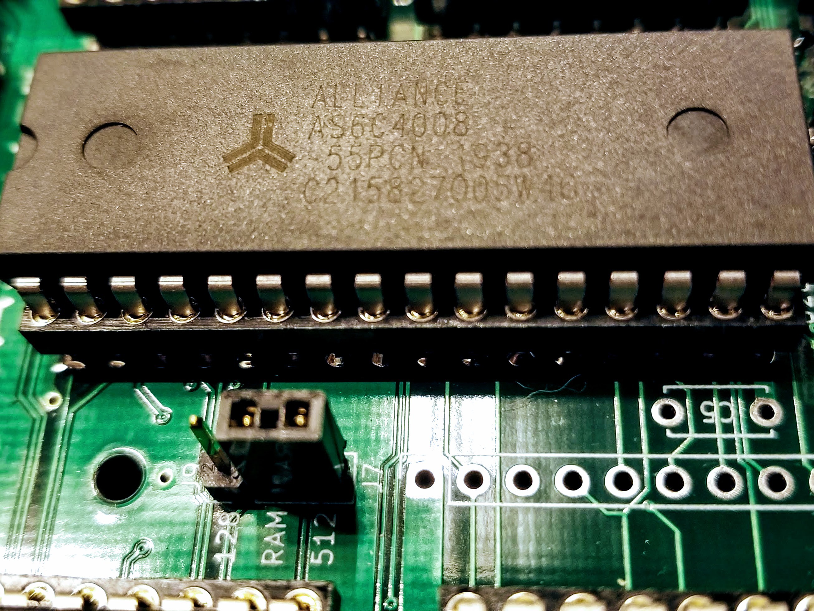
The original design uses 128k RAM divided in to two banks: user and video. The bank is selected by a bit in the instruction, allowing fast switching between these two memory banks. The video memory is the only bank read by the GPU and must always be selected during the GPU RAM cycle. However, the other bank could be further selected and there are up to 3-bits available from the E register to do this.
It was possible to implement this change by swapping a quad 2-input OR gate (74F32) with a quad 2:1 mux (74F157). A lot of things had to get moved around and the board went through a three-week long revision. The layout didn't change much, but almost all the ECU traces had to be rerouted. A jumper (shown below) was added to select between the original 128k and the new 512k memory chip.
![]()
Another change was the power supply. Unfortunately, the high voltage buck converter didn't make it through the final round of Rev. 4 testing. There is over 3 watts being generated in just one cubic inch of space and things were overheating. The temperature is stable if air can flow over the area, but it starts to get too hot once the enclosure is sealed up.
The alternative was a linear regulator, specifically the LDO variety. There are 1.5A versions available that can operate within 0.4V of the input and accommodate a 6V power supply. Like a lot of power supplies, the one currently under test outputs 5% over the rated voltage. There's about 366m ohms between the supply and the regulator dropping this to about 5.75V. The remaining drop across the regulator results in 1.125W being dissipated as heat, almost 1/3rd of the buck regulator design.
The thermal properties of the board are much improved. The minimal board was assembled and tested up to 50C. Not only was it stable, it could run this hot at 35MHz with no decoupling capacitors fitted! This is a first and it appears the changes in the design and PCB layout have all been positive.
-
COSMAC
03/08/2020 at 22:32 • 0 commentsThe hardware abstraction layer contains a virtual CPU for executing application code. The plan has always been to emulate an existing CPU, but which one? 8-bits for sure, and since the Intel-derived CPUs (8085/Z80) were too complex, the initial approach was towards a Motorola-derived CPU (68XX/6502). There is a third option though; the RCA 1802 COSMAC.
This chip is often overlooked because it didn't gain the same visibility as the other 8-bit micros. RCA started its precipitous decline soon after the CPU was launched and their commercial products were all flops. The CPU did find success in the embedded market, from GM's first ECU to space probes.
![]()
The COSMAC is closer to RISC rather than the typical CISC processors of the era. This minimalistic design makes it even easier to implement that the Motorola-derived chips. The chip contains a total of 16 index registers, each with 16 bits, a single 8-bit accumulator, and a few other status registers.
One issue with chips like the 6502 is their register constrained design (they rely heavily on a zero page to expand a limited set of registers). The emulator has access to its own zero page and can implement up to 256-bytes of registers at no additional cost. There is no benefit to implementing a register constrained design. In fact, a lot of 6502 code would be working around this limitation for no reason. COSMAC code tends to work within its own set of registers and this means it works within the emulator's zero page, so is far more efficient virtual CPU.
The COSMAC uses a fetch and execute sequence, with a single fetch, and typically one, or sometime two execute cycles. The 1976 COSMAC CPU would run with a 4-5uS machine cycle, so comparable to the 5.2uS machine cycle of the hardware abstraction layer (HAL).
The fetch code of the HAL just fits in the 43 clock cycles of the virtual machine cycle. There is one caveat: the program counter is pre-incremented. This is the only way to make it fit, so this will break binary compatibility of assembled machine code. However, the code can be easily fixed via static analysis - absolute jump locations need to be reduced by one.
For the fetch cycle, any one of the index registers can be assigned to the program counter (the PC is essentially an indirect address). This address is used to reference the two bytes of the PC in the emulator's zero page. The lower byte is incremented and the upper byte is either loaded or incremented if the lower byte overflows. The memory location at this address is read and copied to an instruction cache in the zero page. This instruction is then used, along with the virtual machine state, to decode the next page jump.
Most of the execution will fit in a single virtual machine cycle, but there are a few exceptions. One is the long branch - this is where the next two bytes referenced by the PC need to be read and then used to update the PC. This requires a double length virtual machine cycle (86-clock cycles).
This is where the indirect location of the PC is used to find and then increment the PC (two step process with conditional jump), load the value at that memory location and then save it in a temporary location. It has to be cached because the PC needs to be incremented again to load the second byte. Both bytes are then used to update the two bytes of the PC (indirectly). This is a lot of work with such limited hardware, as can be seen in the assembly code below:
# Long Branch (LBR)
INCLUDE ../inc/unary.nsa
INCLUDE ../inc/zpage.nsa
INCLUDE ../inc/pages.nsa
PAGE LBR_PG

# $PREG - zero page location of the P register
# $PREG:  10> 100
# $REG0H: 100> 222 Big-endian
# $REG0L: 101> 254
# assume: Y = $VMS
LDZ HL, $INC2$NULL
FNH DZ, HLD        # double inc state
LD HL, $INC$FORK
LDZ Y, $PREG       # zero page address of PC (Y=10, [10]->100)
FNH DZ, Y          # Y = lower byte address (y=101)
FNFH DZ, XD        # inc value of lower byte put in X ([101]->254->255->X)
FNEL A, PC         # fork based on X
#16

ADDR 0x40          # if X=0xFF : iden Y, inc X, inc Y
LD HL, $IDEN$NULL
LDZ Y, $PREG       # zero page address of PC (Y=10, [10]->100)
FNH DZ, Y          # Y = upper byte address (y=100)
FNH DZ, Y          # get value of upper byte put in ([100]->222->Y)
FNFH B, NA         # get value of memory put in A (A=[Y,X]=[222,255])
LDZ Y, $TEMP
FNFH AZ, ND        # store A in temp
#32
LD HL, $INC$IDEN
LDZ Y, $PREG       # zero page address of PC (Y=10, [10]->100)
FNH DZ, Y          # Y = lower byte address (y=101)
FNFH DZ, XD        # inc value of lower byte put in X ([101]->255->0->X)
LD Y, $PREG        # zero page address of PC (Y=10, [10]->100)
FNFL DZ, Y         # Y = upper byte address (y=100)
FNFH DZ, ND        # inc value of upper byte leave in A ([100]->222->223->Y)
LD HL, $IDEN$INC
FNH A, Y           # move A to Y
FNFH B, NA         # get value of memory put in A (A=[Y,X]=[223,0])
#56
LD Y, $PREG        # zero page address of PC (Y=10, [10]->100)
FNFL DZ, Y         # Y = lower byte address (y=101)
FNFH AZ, ND        # save A to lower byte of P (A->[101])
LDZ Y, $TEMP
FNFH DZ, NA        # copy temp to A
LDZ Y, $PREG       # zero page address of PC (Y=10, [10]->100)
FNH DZ, Y          # Y = upper byte address (y=100)
FNH AZ, HLD        # save A to upper byte of P (A->[100])
#75
NOP
NOP
NOP
LD HL, $NOP
LD Y, $VMS         # set Y = $VMS on exit
VMPHL DZ, PGA      # jump to next VMC
#86

ADDR 0x80          # if X=0 : inc Y, inc X, iden Y
LD HL, $INC$IDEN
LD Y, $PREG        # zero page address of PC (Y=10, [10]->100)
FNFL DZ, Y         # Y = upper byte address (y=100)
FNH DZ, HLD        # inc value of upper byte leave in A ([100]->222->223->Y)
LD HL, $IDEN$INC
FNH A, Y           # move A to Y
FNFH B, NA         # get value of memory put in A (A=[Y,X]=[223,0])
LDZ Y, $TEMP
FNH AZ, HLD        # store A in temp
#36
LD HL, $INC$IDEN
LDZ Y, $PREG       # zero page address of PC (Y=10, [10]->100)
FNH DZ, Y          # Y = lower byte address (y=101)
FNFH DZ, XD        # inc value of lower byte put in X ([101]->255->0->X)
LD HL, $IDEN$INC
LDZ Y, $PREG       # zero page address of PC (Y=10, [10]->100)
FNH DZ, Y          # Y = upper byte address (y=100)
FNH DZ, Y          # get value of upper byte leave in A ([100]->223->Y)
FNFH B, NA         # get value of memory put in A (A=[Y,X]=[223,0])
#56
LD Y, $PREG        # zero page address of PC (Y=10, [10]->100)
FNFL DZ, Y         # Y = lower byte address (y=101)
FNFH AZ, ND        # save A to lower byte of P (A->[101])
LDZ Y, $TEMP
FNFH DZ, NA        # copy temp to A
LDZ Y, $PREG       # zero page address of PC (Y=10, [10]->100)
FNH DZ, Y          # Y = upper byte address (y=100)
FNH AZ, HLD        # save A to upper byte of P (A->[100])
#75
NOP
NOP
NOP
LD HL, $NOP
LD Y, $VMS         # set Y = $VMS on exit
VMPHL DZ, PGA      # jump to next VMC
#86

ADDR 0xC0          # if else : iden Y, inc X, iden Y
LD HL, $IDEN$NULL
LDZ Y, $PREG       # zero page address of PC (Y=10, [10]->100)
FNH DZ, Y          # Y = upper byte address (y=100)
FNH DZ, Y          # get value of upper byte put in ([100]->222->Y)
FNFH B, NA         # get value of memory put in A (A=[Y,X]=[222,255])
LDZ Y, $TEMP
FNFH AZ, ND        # store A in temp
#32
LD HL, $INC$IDEN
LDZ Y, $PREG       # zero page address of PC (Y=10, [10]->100)
FNH DZ, Y          # Y = lower byte address (y=101)
FNFH DZ, XD        # inc value of lower byte put in X ([101]->255->0->X)
LD HL, $IDEN$INC
LD Y, $PREG        # zero page address of PC (Y=10, [10]->100)
FNH DZ, Y          # Y = upper byte address (y=100)
FNH DZ, Y          # get value of upper byte leave in A ([100]->222->Y)
FNFH B, NA         # get value of memory put in A (A=[Y,X]=[223,0])
#52
LD Y, $PREG        # zero page address of PC (Y=10, [10]->100)
FNFL DZ, Y         # Y = lower byte address (y=101)
FNFH AZ, ND        # save A to lower byte of P (A->[101])
LDZ Y, $TEMP
FNFH DZ, NA        # copy temp to A
LDZ Y, $PREG       # zero page address of PC (Y=10, [10]->100)
FNH DZ, Y          # Y = upper byte address (y=100)
FNH AZ, HLD        # save A to upper byte of P (A->[100])
#71
NOP
NOP
NOP
NOP
NOP
NOP
NOP
LD HL, $NOP
LD Y, $VMS         # set Y = $VMS on exit
VMPHL DZ, PGA      # jump to next VMC
#86
There's a lot going on in that code, but the main structure revolves around the FORK function. The first step is to increment the lower byte of COSMAC PC (referenced by the value in the zero page at $PREG). The result of this increment is loaded in to the X register and passed to the FORK operation. This then jumps to one of the following locations in the page:
- 0x40 if X=0xFF
- 0x80 if X=0x00
- else 0xC0
The code in these three sections then handles the necessary incrementing of Y to reference the following memory locations:
- 0x40 - read [Y, X], read [Y+1 ,X+1]
- 0x80 - read [Y+1, X], read [Y+1, X+1]
- 0xC0 - read [Y, X], read [Y, X+1]
The rest of the code is basically the same in each section. The optimization is having the FORK take care of all the conditional jumping in a single step.
Novasaur CP/M TTL Retrocomputer
Retrocomputer built from TTL logic running CP/M with no CPU or ALU