Alastair Hewitt
-
One Year Later
02/27/2020 at 20:14 • 3 commentsIt was a year ago when I stumbled across the infamous 8-bit Guy video demoing the Gigatron. I was working on a retro arcade cabinet at the time, but building a video game system from scratch was a much more interesting challenge. It wouldn't be the first time either. I built a Racer game out of TTL chips using a 7x7 LED matrix as a senior project at school. I then spent that summer working on a Harvard Architecture CPU with a ROM-based ALU. I never thought about generating VGA (it was still a couple of years away at the time) but seeing the Gigatron achieve this with so little has re-inspired me!
![]()
I'm essentially at the same place I was almost 12 weeks ago: I can copy an image from the ROM to the video RAM and generate the video timing. What has changed is the way the video timing is generated and how this code is built.
The initial code was developed old skool by assembling the machine code by hand and then typing the hex code into the WIndows app that came with the EPROM programmer. It was nostalgic, but not very productive (not to mention frustrating when you typo '6' instead of 'b').
The project now has an assembler and a build script to compile the code, calculate the ALU lookup tables, and generate fonts. The final step of the build process is to flash the ROM image using minipro. There is no simulator though, so testing must be done on real hardware and debugging still requires an oscilloscope.
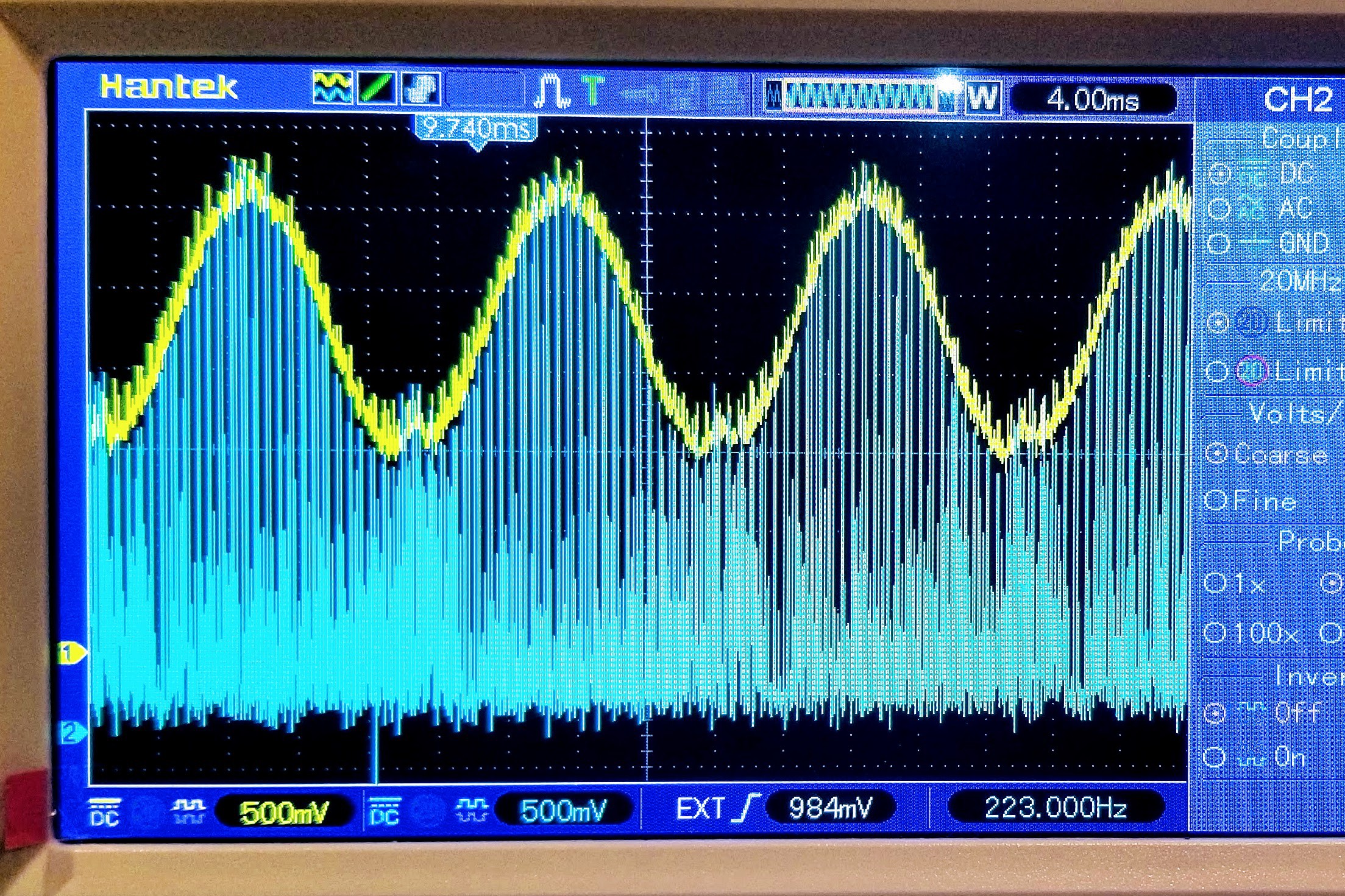
The oscilloscope trace above shows the Page Register clock pulse occurring every 52uS. This represents the virtual machine clock of a hardware abstraction layer developed over the last few weeks. This is the foundation of the system going forward and will be providing video, a virtual UART, "sound chip", and CPU for an operating system and user applications.
Hardware Abstraction Layer
There are multiple systems on the board with timing critical requirements like the video, audio, and serial ports. A user program can not take control of the hardware without having a significant insight in to the various timing constraints and requirements of these systems. The solution is to put an abstraction layer between the hardware and user program.
Even though this has drifted up and down a bit, the final dot clock (until it changes again!) is 33 MHz. This drives a 4-phase clock for the hardware process clock of 8.25MHz. The hardware abstraction layer divides this clock down to a 43-cycle fixed virtual machine cycle running at 191.86kHz. This is further divided down to 9.593kHz by using 20 machine cycles to create a virtual process cycle consisting of either 4 lines of 5 cycles, or 5 lines of 4 cycles.
Each line in the process cycle ends with a single machine cycle dedicated to timing. This cycle updates the scan register to generate the video sync pulses, updates the V register to select the next line for the GPU to render, samples the serial ports, and decides what additional cycles are needed to handle features (audio and serial communication).
The remaining cycles are available to execute user code on a virtual CPU. So the 4-line process cycle has 16 machine cycles (153,488 per second) and the 5-line process cycle has 15 machine cycles (143,895 per second) to execute user code. The virtual CPU uses a fetch/execute cycle, where the execute would need at least one and sometimes two machine cycles. The average would be around 2.3 cycles per instruction, which equates to a virtual CPU speed of around 66k instructions per second.
Video
The ALU now contains a video timing function to support four video timing schemes. The first two use the 4-line virtual process cycle with a horizontal frequency of 38.372kHz. The first of these uses 128 process cycles per field to generate VGA at 75Hz (VESA DMT ID: 06h). The second uses 160 process cycles per field to generate SVGA at 60Hz (VESA DMT ID: 09h). The last two timing schemes use the 5-line virtual process cycle with a horizontal frequency of 47,965kHz. These both use 160 process cycles per field, with the first generating XGA at 60Hz (VESA DMT ID 10h) and the second supporting the latest VESA CVT reduced blanking v2 (CVT 1.01MA-R).
There are 8 ways to divide down the vertical timing in the 4-line cycle modes (VGA/SVGA): divide by 2, 3, 4, 5, 6, 8, 10, 16. The divide by 2 and 3 are normally used for hi-res graphics (bitmapped, 8 colors). The divide by 4, 5, and 6 are used for lo-res graphics (bitmapped 256 colors), and 8, 10, and 16 are used for the text modes. The 5-line cycle (XGA) can only fit 6 ways: 3, 4, 6, 8, 10, 16.
There are also three hardware bits to control the GPU: mode1 - 1 or 2 cycle timing (used to select text vs graphics mode), mode2 - video DAC (8 or 256 colors), mode3 - reduced blanking on/off (only used for CVT).
A single byte is used to define the video mode, but only 7 bits are needed. There are a total of 112 addressable video modes. Some are not too useful, but many of these are. In general there will be hi-res/lo-res bitmapped graphics and normal or compressed text modes in either 4:3 or 16:9 aspect ratios.
One final note on the horizontal resolutions. The 33MHz dot clock is close to the native clock of the 75Hz VGA timing to render the standard 640 resolution. The other timings expect a faster dot clock that will render as a lower horizontal resolution. The 33MHz dot clock is about 80% of SVGA and will also render with a resolution of 640 (80% * 800), but only to 512 in XGA (50% * 1024). Both the VGA and SVGA modes support 80 column text, but XGA is closer to 64. However, the final mode uses CVT timing with reduced blanking (only supports newer LCD monitors). The ALU timing function generates timing for a 1295 x 777 at 60Hz mode assuming a 66MHz dot clock. This is exactly twice the actual dot clock so the rendered resolution is now close to 640 and can also support 80 columns of text.
Serial
There are two serial ports and each one has two bits in and out. One port is used to communicate via the RS232 interface and the other supports the keyboard. This is where the specific frequency of the virtual process cycle also comes in to play. The process cycle is aligned to support communications at a 9600 baud rate with the transmission of one bit per process cycle.
The sync code for the video timing only uses about half the 43 hardware process cycles leaving the other half to process the incoming serial stream. Another custom ALU function is used to sample the serial inputs and drive a state machine. The final state determines if and what data was received over the ports at the end of the virtual process cycle.
The data input of the RS232 interface is more or less aligned with the virtual process cycle, but will drift slightly. Sampling over more than one line can identify the drift and compensate to determine the value of the input bit correctly.
The keyboard is a little more complex. The PS/2 interface generates its own clock and this frequency is defined over a range of 60-100uS. The virtual process cycle is 104uS, so one or two bits could be sent in a single cycle. The state machine outputs two values to determine if zero, one, or two bits were received and their value.
Both serial ports have hardware flow control and even though the serial interface is sampled all the time, the serial communication is a feature that is turned on/off. When turned on the output of the serial sample state machine is processed by an additional machine cycle during the process cycle.
Audio
There are no resources dedicated to the audio unless the audio is turned on as a feature. When turned on an additional machine cycle is used to handle the audio state and then one machine cycle is required per voice, up to a total of four voices. Each voice is sampled once per process cycle, at a rate of 9.6kHz. This limits the highest frequency to 4.8kHz, but is high enough to support the full 88-key piano scale.
CPU
Work is currently underway to implement a binary compatible version of the RCA 1802 COSMAC microprocessor. This is a huge subject in its own right, so I won't go in to the details here. One thing to note with this design though. The virtual machine cycle will map almost 1:1 with the COSMAC machine cycle. The COSMAC required 8 clock cycles per machine cycle, so the hardware abstraction layer is running at the equivalent of 1.23MHz, or about 70% as fast as the COSMAC Elf/Pixie.
-
Happy New Year!
01/25/2020 at 02:51 • 0 commentsAs in the Chinese Lunar New Year! It's remarkably cheap to run prototype PCBs since the design works on a 2-layer board. I decided to ship the Rev. 3 board design last week to get it here before things shut down in China.
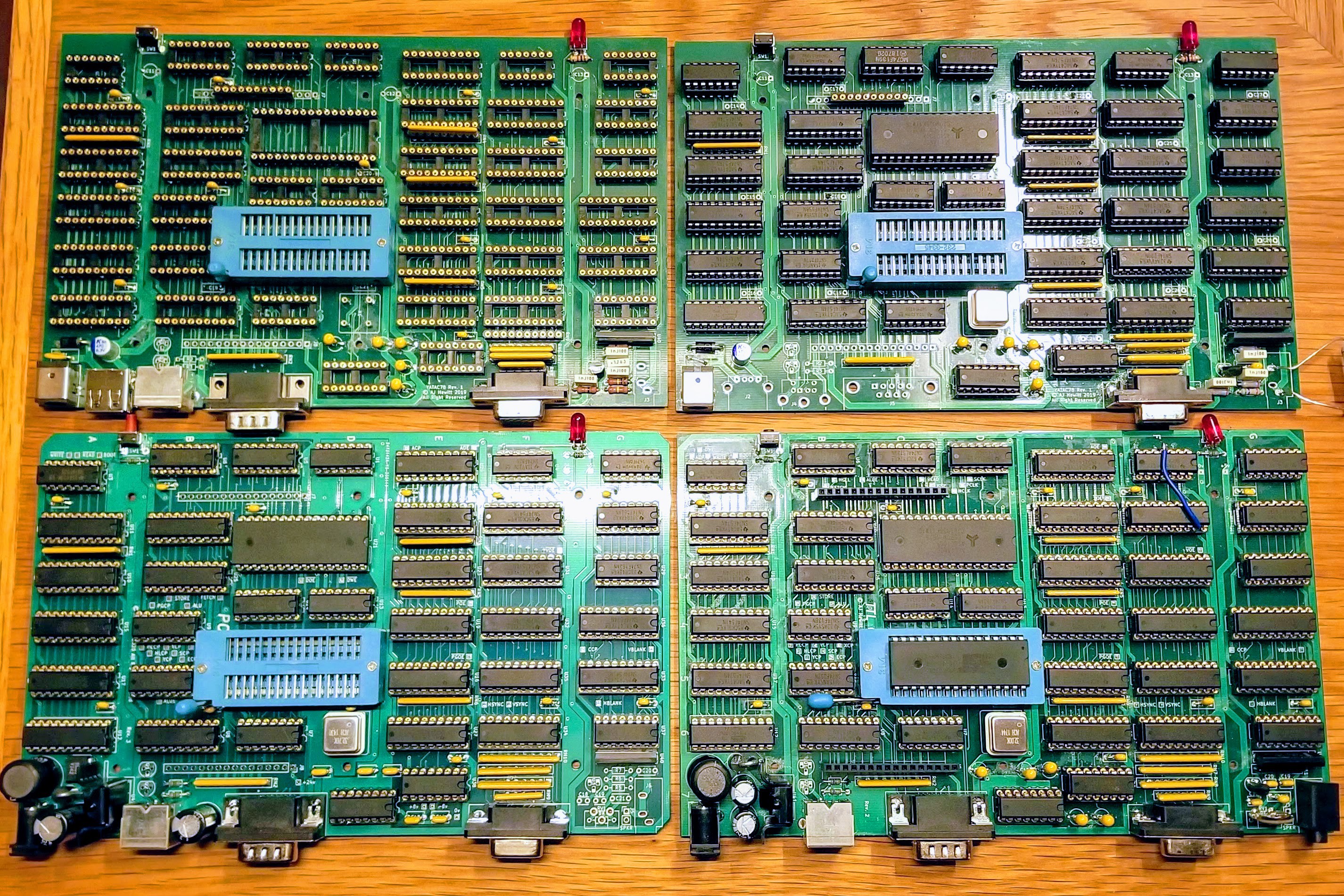
![]()
There's now four populated boards (2x Rev. 1 boards on top, Rev. 3 and Rev. 2 on the bottom of the picture)
Rev. 3 included a few minor updates to improve the ground planes and power distribution. A bridge rectifier was added and the filter capacitors were increased to handle AC power input. There was also an update to the horizontal control circuit to allow switching between 2 and 3 micro-second H-sync pulses.
The good news is the board worked first time. The bad news was the updated power supply generates too much noise when the components heat up. This is not a surprise though. Trying to put the entire power supply circuit on the same board was really pushing it!
The output filter cap was moved away from the main switching circuit due to space constraints. This adds inductance to the ground return path and increases the switching transients on the buck regulator. This causes sharp 20ns pulses riding on the power lines and some pretty horrifying EMC implications I would imagine. The board starts ok, but then becomes unstable as the thermal drift kicks in.
The Rev. 2 buck converter is working fine though, so the power circuit will be rolled back for the Rev. 4 board. Further testing seems to indicate a 33MHz dot clock is going to be stable and the the hardware abstraction layer is being designed around this (more on that in a later log). The true color video output is greatly improved in terms of supply noise. Not only that, but the video signal gets cleaner as things warm up. There's something strangely satisfying about that in a vacuum tube sort of way.
-
If It Ain't Broke, Don't Fix It
01/05/2020 at 18:19 • 0 commentsThere was one final delta between Rev. 1 and 2: The H-sync was put through the bus control latch to align it with the dot clock. This wasn't really necessary, so was rerouted to be a straight connection on the Rev. 2 board. This frees up a flip-flop for use elsewhere and was used to resample the output enable of the X register. However, this required an additional shift in the clock phase that was not made. The result was bus contention on the lower part of the RAM address.
It's surprising the board was able to run at all with this problem. The OTP ROM did not work because it contained the text fill code and this was crashing before the video loop could start. The problem was resolved by cutting a pin and using a patch wire to select the correct clock phase.
![]()
The Rev. 2 board is working and was able to run with the 35MHz dot clock. The quality of the video signal is greatly improved with the cleaner supply lines. The assumption was the cleaner supply would also improve the stability at 35MHz, but things are starting to glitch as they warm up. Dropping to 32MHz resolves any remaining stability issues and this is likely be the final dot clock speed.
There's not much more to test on the computer side of things, so testing is focusing on the new power supply design. A trip to the local electronic store to pick up more solder lead to a chance discovery. They had inexpensive linear power supplies. I don't need a regulated input and a big hunk of iron in the power supply has additional retro appeal. Another option is to add a bridge rectifier to the the board to support an AC input. This would only require a simple iron core transformer for the power source.
![]()
-
One Step Forward, Two Steps Back
01/04/2020 at 05:17 • 0 commentsThe Rev. 2 PCB came in yesterday and the first sample has been built and tested. The image below shows the Rev. 1 (left) and Rev. 2 (right) boards. The plan is to keep one fo the previous revisions of the board on hand to compare in the case the new revision is a step backwards... which unfortunately appears to be the case here...
![]()
The biggest delta between the two revisions was a new power distribution layout including a cooper pour on the back for a ground plane. The Rev. 1 board needed a few patch wires to add additional ground return paths. These problems should be eliminated on the new board and so far the power lines do look a lot cleaner.
![]()
The new board booted up first time and flashed the blinkenlight on and off at the correct 1Hz frequency. The V-sync signal was glitchy and prevented the video from syncing. Dropping the dot clock to 32MHz fixed the issue and the board appears to be completely stable at this speed. This was with the slower NOR flash ROM though, so the faster OTP ROM was tested. This didn't work at all... at any frequency, so something is definitely not right.
The other major change was the new on-board buck converter. This is working well and provides a clean and stable 5v supply with up to 2A from a lower current 500mA 24v input. The PCB has the wrong footprint for the regulator with the pins staggered the other way (there will definitely be a Rev. 3 board!). The pins were re-bent and everything was able to fit within the one-cubic inch of available space. The regulator and inductor run hot, as expected. The design calculations indicated a 50C rise above ambient under load and this appears to be the case.
![]()
The final delta was some updates to the audio circuit. The op-amp was tested under load during the Rev. 1 phase and can easily supply up to 150mA. This is enough to drive a small internal speaker, similar to the old UK home computers from the early 80's (ZX Spectrum, Jupiter Ace, BBC Micro, etc). This is optional and would be supported with a speaker connector and trimmer pot to control the volume (once the correct vertical mounted POT is installed). A fixed resistor can be added in place of the trimmer for a line-level output from the audio jack.
![]()
So there's some debugging ahead to work out why the faster clock is not working and why the OTP ROM doesn't work. It's possible that both issues are related, but figuring out the root cause is likely to burn up the entire weekend.
-
Expansion Board
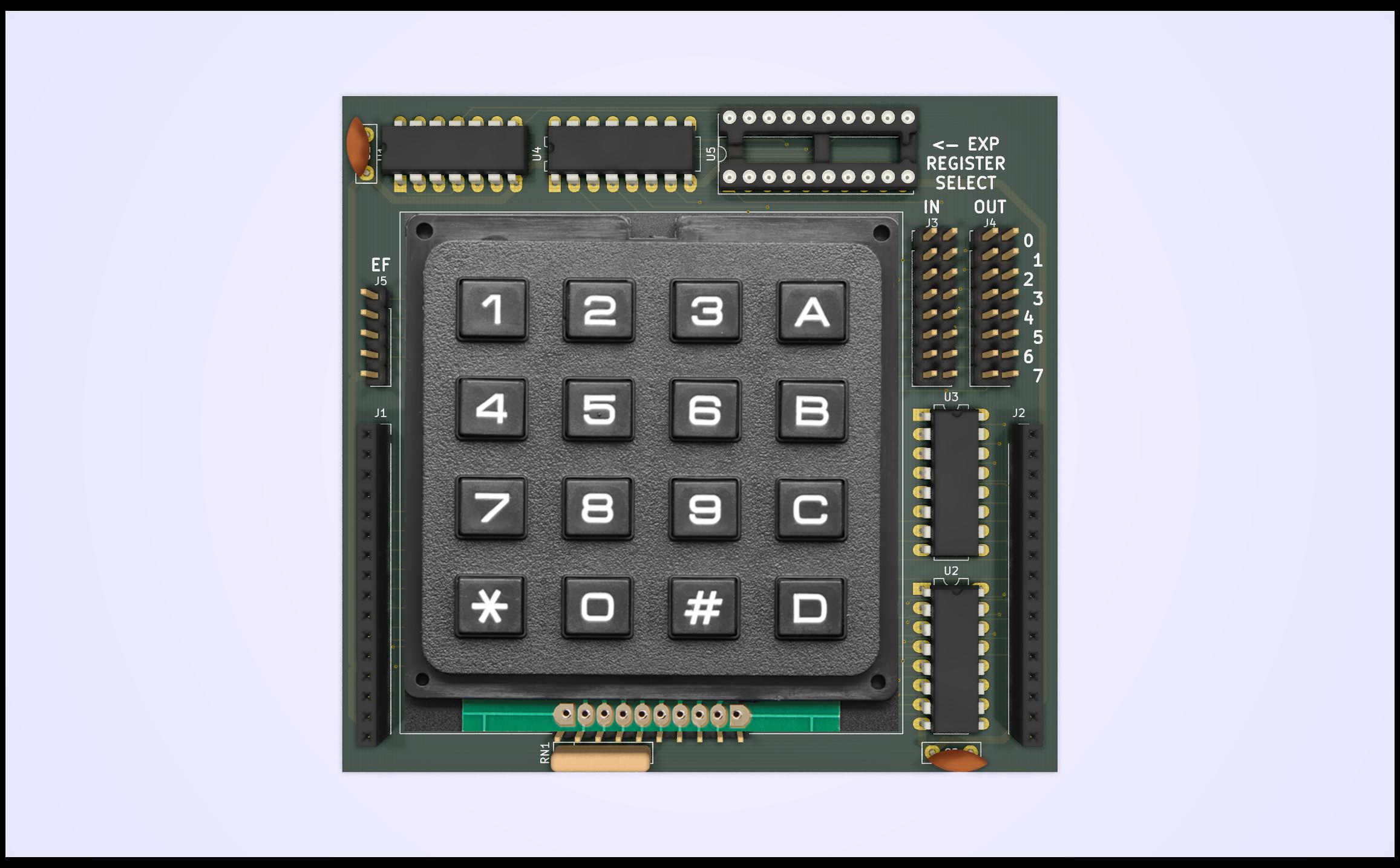
12/26/2019 at 21:07 • 0 commentsAn expansion method was an important feature of the design and provisions were put in place to allow data a parallel data path in and out of the system. The current design is aligned to support the RCA 1802 (COSMAC) with up to eight input and output registers, four external flag inputs (EF), and a single flip-flop output (Q).
Two 16-pin headers are installed on the main PCB to expose the two data busses and a minimal set of control signals. From here only two 3-to-8 decoders and a 4-bit buffer is needed to complete the expansion interface. These components are not included on the main PCB since the expansion is optional and not needed for normal operation.
![]()
A simple expander card has been designed in order to test this interface and will be manufactured alongside Rev. 2 main board. The expander is typically 10cm x 10cm in size (the threshold for the lowest price tier for most PCBs) and mounts over the main PCB like a shield.
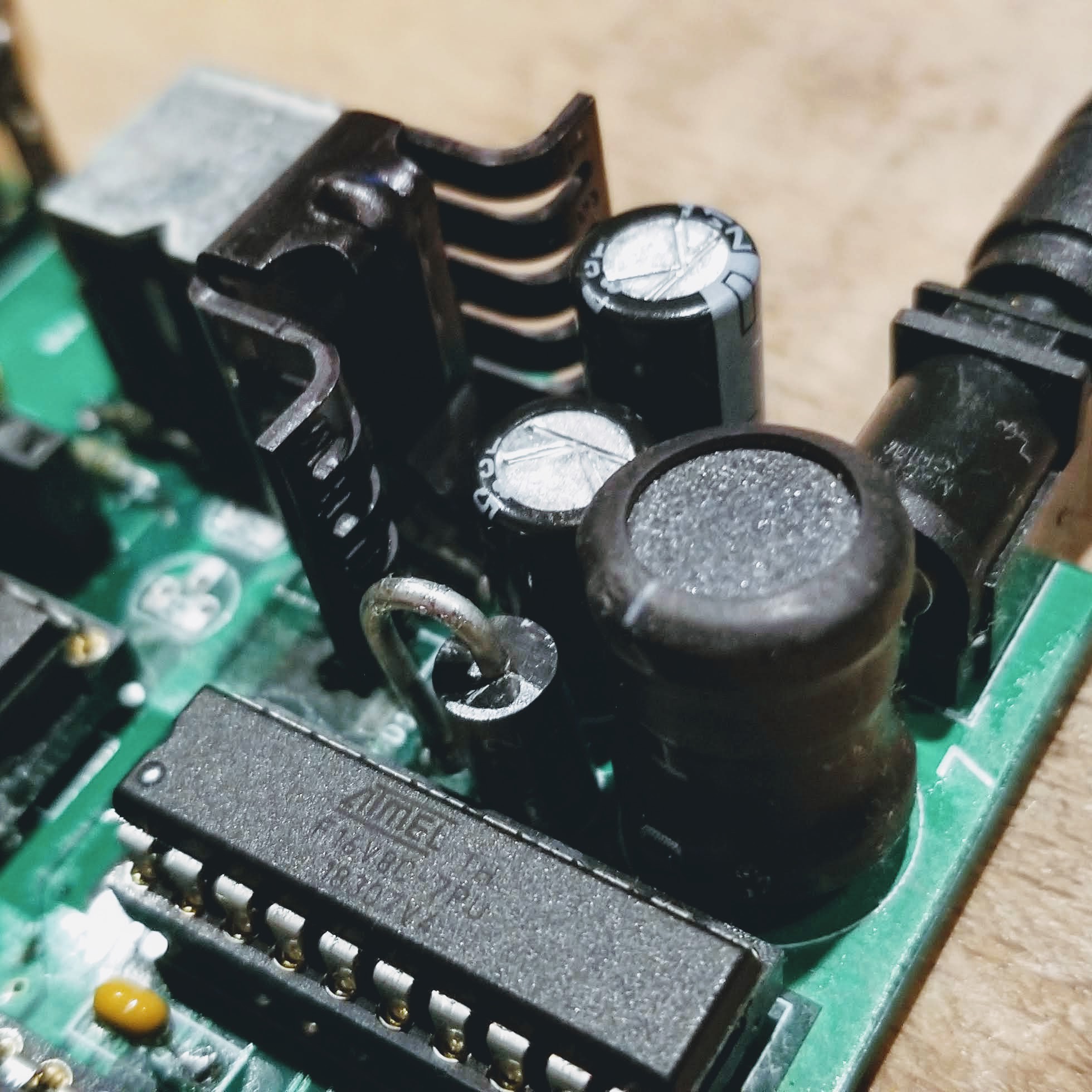
The design includes a socket for a single 8-bit expansion register. Two sets of headers with jumpers allow this register to appear as any one of the eight possible input and/or output registers. An additional set of four flip-flops is included in the 7th register position and can be used to scan a 4x4 keypad matrix with the return 4-bits going to the expansion flags (EF).
The keypad is just a temporary measure for testing and will not be needed once the PS/2 keyboard serial code is built and working. That could be up to 6 months away though.
-
Audio
12/19/2019 at 05:00 • 0 commentsNot much has been said about the audio yet, but it's definitely a feature and currently being tested.
![]()
First a quick overview of the zero page to better understand how the audio system works. A zero page is typically the first page of the memory and only requires a single byte to address one of 256 possible values. In this design the zero page is put in the upper bank of memory along with the display. The display uses all the pages of this memory, but only the first 209 bytes of each. To accommodate this the zero page is oriented to be the last byte of each page. So rather than setting the Y index to 0 and using the X index to address the zero page location, this design sets the X index to 0xFF and uses the Y index to address the location.
The 0xFF value for the X register is created by adding pull-up resistors to the address bus and leaving the X register in tri-state during the zero page access. A similar approach is used with the GPU where both the H and V registers are left in tri-state during the horizontal blanking period. This selects not only the zero page, but the very last byte at the top memory address of 0x1FFFF. This last byte of the zero page is used to store an 8-bit audio sample.
So during the horizontal blanking period the GPU reads the audio sample and puts it on the lower 8-bits of the ROM address bus. Normally the GPU context selects the font area of the ROM, but in the horizontal blanking period the ALU context is used. Not only that, the upper ROM address is also left in tri-state and pull-up resistors select 0xFF of the ALU. This selects the unary identity function and passes the value of the audio sample through the ROM unaffected to the glyph register.
The glyph register does double duty: It acts as a pipeline for the glyph line while colors are loaded, but during the blanking period it holds the audio sample read from the zero page. An audio DAC is added in the form of an R2R resistor network to output the analog version of the audio sample during the blanking period. The audio DAC output is only sampled during the blanking period to reject the video signal during the non-blanking period. The sampled signal is then filtered to remove the high-frequency and DC components.
To test the audio a sine wave was added to the ROM and addressed by the video vertical line address. This results in a sine-wave at the video field rate of 60 Hz and sounds exactly like electrical hum :) One issue identified is with the sample and hold circuit. This currently uses a BS170 MOSFET with a threshold voltage of only 0.8v and this is not completely turning off on the bottom half of the cycle. The image below shows the sine wave transposed up but still experiencing some breakthrough of the video signal during the bottom part of the cycle. Switching to a BS270 may fix this, but further investigation is ongoing.
![]()
-
Power Supply Design
12/11/2019 at 22:51 • 0 commentsThe remaining instability in the Rev. 1 board is down to power issues. The power distribution was deliberately underspecified to highlight problem areas and test different designs. There are two main areas of concern: inductance and current consumption.
Inductance is the biggest enemy for maintaining a clean power supply. The decoupling capacitors help, but adding multiple return paths to ground seems to be the most reliable strategy. The inductance of each path is placed in parallel, so two paths will halve the inductance of the single path.
![]()
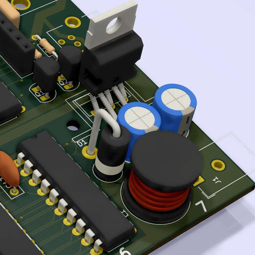
Inspiration was taken from 70's video game boards (an example shown above). These were designed before the introduction of microprocessors and typically required well over a hundred (non-LS) TTL chips. These are arranged in columns of several chips with one or more decoupling capacitors per column and a dual return power path. This is the approach taken for the power distribution on the Rev. 2 board.
![]()
The other issue is the relatively large current consumption at 1.5A. This is just for the core system and doesn't include additional power to things like a WiFi dongle (2W) or expansion board (300-500mA). This pushes the maximum current consumption closer to 2.5A and poses some major challenges in maintaining the supply voltage between 4.75v and 5.25v
The initial plan was to use a 5v power adapter and there are plenty of inexpensive options to meet the current requirements. The problem with these is the resistance between the power supply and the power distribution on the board. The leads from the supply and resistance of the barrel jack connector comes in over 300 milli-ohms. This would drop the voltage by 0.75v at 2.5A, resulting in only 4.25v getting to the board power rails. Some 5v supplies output 5.25v to compensate, but this still means the supply would only reach 4.5v on the board.
One idea was to start with a higher voltage like 6v and add some additional resistance to drop the voltage down to 5v. The 6v supplies also tend to compensate and typically output 6.3v, so adding a 0.22 ohm power resistor to the supply line would drop the voltage to 5v (assuming a total resistance of 520 milli-ohms). This assumes a current consumption of 2.5A, but the base system consumption of 1.5A would result in a supply of over 5.5v if the additional components were not used with this approach.
What's really needed is a regulator on the board. One option is a linear regulator to take a 9v or 7.5v supply and drop it down to 5v. Again the current consumption poses a problem here resulting in up to 2.5W of heat dissipation for each volt dropped. Low-dropout regulators are available, but these would still result in over 4W of dissipation and require a large heatsink. The other option is a buck converter and this is the current plan for the Rev. 2 board.
There are inexpensive SMD modules that can fit in the available space, but these don't have the best thermal design or reliability. The components are available in through-hole however and the buck converter can be added directly to the board. A small heatsink is required and this can be wrapped around one of the mounting holes to maximize the available space as shown below.
![]()
This design can use a much higher voltage and avoid the large input current and voltage drop getting the supply to the board. The current power supply design would only need 600mA using a 24v supply. This includes 2W of direct power to the Wifi dongle and provide up to 2A at 5v via the buck converter for the main system and optional expansion board (assuming 80% efficiency). Heat dissipation is also a more manageable 2W with this design.
-
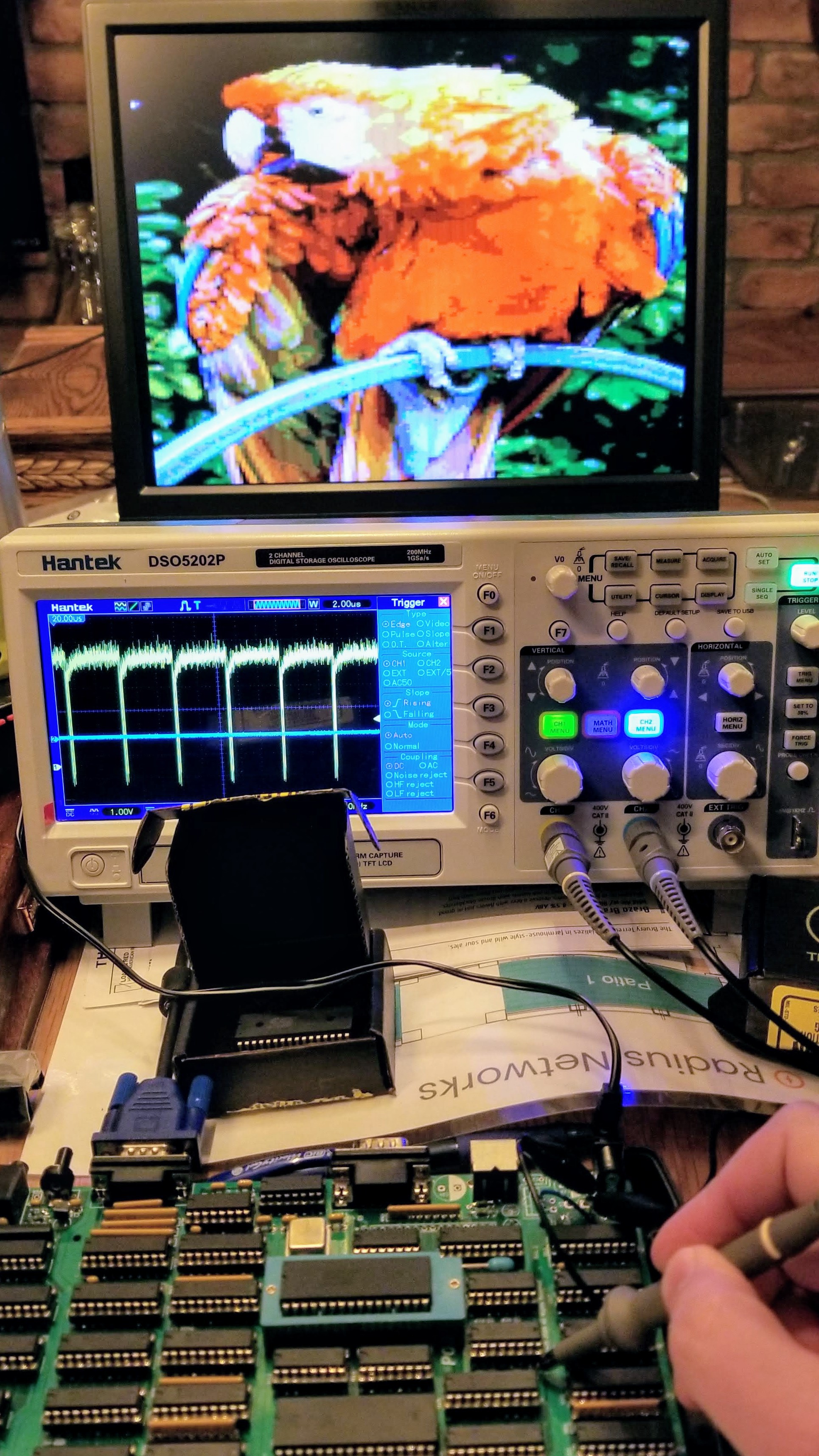
Parrot!
12/08/2019 at 05:04 • 1 commentOne significant milestone in any home brew VGA project is to generate a parrot image... so here it is!
![]()
This is in the lo-res video mode (160x120) using the 3:3:2 video DAC. To do some baseline testing the board generating this does not have any decoupling capacitors and it looks pretty terrible. The video is being oversampled by a factor of 5 and a lot of the supply noise shows up in the image (the white area below should be the same color).
![]()
Hopefully this will be greatly improved with the Rev 2 board, which is where most of the time over the last 2 weeks has been spent. Also worth noting is how this image is generated. The image is stored in the ROM, but the Harvard Architecture prevents data from being read from the ROM. The image is actually the product of several ALU functions, each one acting as a lookup table to return parts of the bitmap image.
-
HDMI Test in SVGAish Mode
11/28/2019 at 03:35 • 0 commentsA quick test with the video loop updated to SVGAish mode. The differences being the 35MHz dot clock is 7/8th the speed of the true SVGA 40MHz clock. This means 87.5 columns of text instead of 100.
![]()
The horizontal frequency is also adjusted up slightly from the SVGA 37.879kHz to 38.377kHz. This is only a few hundred ppm away from the 38.4kHz UART speed. The TV is happy with this timing passed straight through the cheap $8 VGA to HDMI converter.
-
Initial Rev.1 Board Results
11/24/2019 at 17:46 • 2 commentsThe Rev.1 boards came in earlier this week and a couple where built and tested. The only firmware that exists generates a text mode video pattern, so some unrelated components were not fitted.
![]()
It took a few hours to resolve a couple of issues with the PAL. The pins were reassigned on the PCB version, but the old JEDEC file had been programmed. The reset input shouldn't need an external pull-up resistor, but the PCB version appears to need one. This was patched on the back of the board.
The test program worked first time once the PAL issues were resolved. "Worked" as in it generated a somewhat glitchy test pattern and only with a 25MHz dot clock. This was not encouraging, since this is a similar performance level to the breadboard. Several hundred pads were soldered on the board and this resulted in a lot of flux. This was cleaned off as a precaution, but didn't seem to change anything.
Some initial probing started to identify the source of the problems. The power lines to the chips were showing a decent amount of noise. The board being probed did have decoupling capacitors, but these seemed to be less effective than just using a low inductance path to ground instead. Almost all the glitching was eliminated by adding a single ground return from the RAM chip to the lower power bus.
![]()
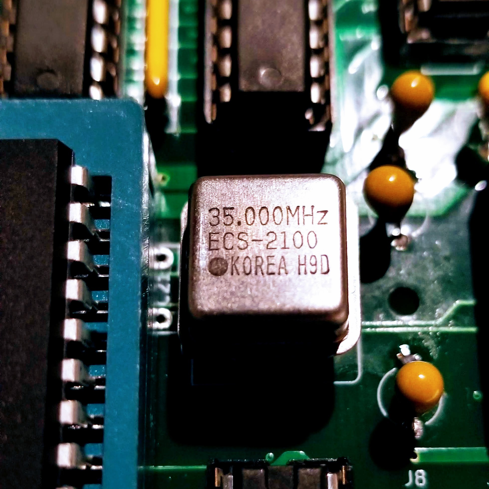
After that the clock speed was retested and the board was now able to reach its maximum dot clock speed of over 36MHz. The closest available oscillator is 35MHz and this was tested to good effect. This results in a machine clock of 17.5MHz and a memory access cycle of 57ns. Both the NOR flash and OTP ROMs respond in about 50ns, so there's 7ns left in the memory access cycle. A 40MHz oscillator was also tested, but there's no time left in the cycle to meet the setup times and latch valid data. The board may go a little faster (36.864?) but the current 7ns buffer is a good place to stop.
![]()
Things were close, but not quite there. One final discovery appears to have cleared up the remaining glitches though. The dual 2-4 decoders are obsolete in the 74F series, but I was able to pick some up on Ebay and I've been using these. I want all the parts to be in production and the design should work with the currently available 74ALS139. This chip is routinely tested to make sure the board will still work and it appears that changing to this version solves all of the remaining glitches. Like many NOS chips listed on Ebay, the 74F139 chips I bought may have come from a rejected batch. It's also possible these 1987 chips have deteriorated over the past third of a century... Either way it looks like the board is now 100% working!
Things are now blocked on further hardware testing until more firmware is written. The two bitmap graphics modes need testing (building out the 8-bit video DAC), the audio system and amplifier/filters, and the serial - both keyboard and RS232. All these require new code and that code will require build tools. Once the rest of the hardware testing is complete a Rev.2 board can be built to rework the grounding issues.
Novasaur CP/M TTL Retrocomputer
Retrocomputer built from TTL logic running CP/M with no CPU or ALU