Alastair Hewitt
-
Firmware
09/02/2019 at 20:08 • 0 commentsA lot of progress was made over the past month on the software side of things. This is a very significant part of the overall system and has also been driving changes in the underlying hardware. A workable design is now in place and some details are covered in the following log.
First, some terminology
- Firmware is used to describe the code that is executed by the machine. This code resides in the ROM and is executed directly by the hardware.
- Software is used to describe the interpreted code that resides in the RAM. This code is read by the firmware and executed to emulate the operation of a virtual CPU.
The firmware is technically running on a RISC machine, except instructions take more than one clock cycle to execute. This is due to the limitation of 8-bit wide memory and putting both the firmware and ALU in the same ROM. The machine could operate at one instruction per clock by using a 16-bit wide memory for the firmware and a separate ROM for the ALU. However, the current design requires up to four cycles per instruction:
- Fetch - one or two process cycles
- Execute - one or two process cycles
Each process cycle consists of two machine cycles which alternate between access to the ROM and RAM. The fetch cycle provides a read access to the RAM and the execute cycle provides an optional write. This way every instruction can take the form: fetch, read, execute, write (the same read and write cycle is repeated when more than one cycle is needed to fetch and/or execute).
The software is interpreted by an emulator in firmware that also controls both the video display and serial communications. These systems are timing critical and maintaining synchronization is a significant part of the design challenge. One approach is tracking the number of cycles per instruction before the synchronized event and breaking when not enough cycles are left to guarantee the next instruction will execute in time. The other is to break the virtual instructions down in to fetch and execute cycles and use fixed cycle timing for each.
Cycle counting makes sense only if the complete instruction fetch/execution time is fairly small. After implementing instruction from various CPUs it appears cycle counting could result in only one instruction being executed between the horizontal sync events. This happens when the first instruction loaded is on the longer side and there isn't enough time left to execute another long instruction. The fixed fetch/execute timing has the ability to split instructions across the horizontal sync event and avoid wasting unusable cycles when longer instructions were executed.
The fixed fetch/execute timing is being used with a processing rate of 9600 cycles per second. This leads to the following counts for vertical video synchronization:
- VGA - 128 process cycles per field at 75 fields per second
- SVGA - 160 process cycles per field at 60 fields per second
Each process cycle consists of 4 lines and each line consists of 5 machine cycles (20 machine cycles per process cycle). One machine cycle is needed per line to perform the horizontal sync at a rate of 38.4 kHz. Three additional machine cycles are used every process cycle for other overheads including serial communication at 9600 baud. This leaves 13 machine cycles for the interpreter, which would equate to around 125k machine cycles per second (average 8 uS per machine cycle). This is equivalent to an RCA CDP1802 running at 1 MHz, or about half the processor speed of the COSMAC Elf.
The machine cycle is tracked using an 8-bit state machine in firmware. This state is combined with the fetched instruction to determine the code page to load via a decode function in the ALU. The state is also combined with the process cycle count via another ALU function to set the Scan Counter. Other custom ALU functions are used by the interpreter such as the Arithmetic Status (AS). This function returns two nibbles, one consisting of the status flags on addition and the other on subtraction. This can be used to update a status register in the absence of a real ALU with status flags built in.
-
CPU State Machine - part 2
08/22/2019 at 04:31 • 0 commentsThe CPU state machine was introduced early in the project and has undergone some evolution as the design progressed. Hopefully things are stable enough to expand on the details.
The CPU essentially does the same thing on every instruction cycle: It fetches an instruction and then latches data from the ROM in to a register. The instruction always comes from the program bank of the ROM, the data can come from either the program half or ALU banks. In the case of the program bank, the data would be an operand. The ALU banks return the result of an arithmetic or logical operation.
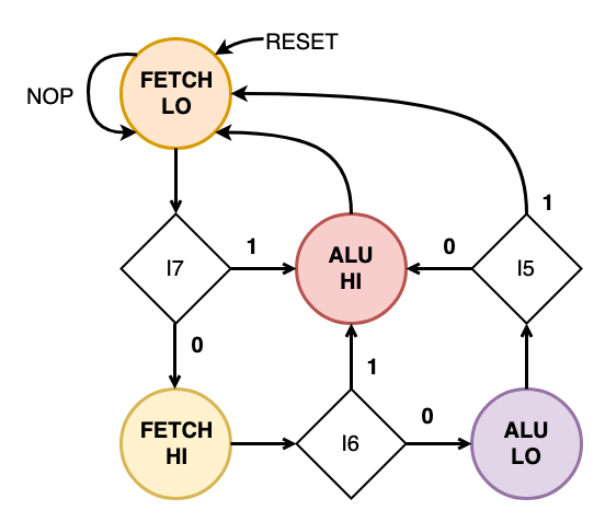
Every instruction cycle begins with an instruction fetch, which can be either one or two bytes in length. The upper bit (i7) of the first instruction byte determines if another instruction byte should be fetched. Once the instruction is fetched an operand or ALU result will follow. In the case of the ALU, either the H or L register can be selected as the input to the ALU, or in the case of 8-bit operations, both the H and L are used sequentially. A conditional option also exists where the operand fetch can be skipped based on the sign of the accumulator. If the condition is not met then the CPU will skip the second part of the cycle and fetch the next instruction immediately.
If any of that made sense then you'll be aware of 4 possible sequences:
- Single Cycle - conditional operand fetch where condition is not met (NOP)
- 2-Cycle - Single byte instruction, fetch operand, or 4-bit ALU operation.
- 3-Cycle - Two byte instruction, 4-bit ALU operation.
- 4-Cycle - Two byte instruction, 8-bit ALU operation.
This state can be handled with a 2-bit finite state machine. The op code is encoded using the top 3-bits of the first instruction byte (i7-5). Only the H register is used for the 2-cycle ALU operations and is also used when i6 is high in the 3-cycle operations. If i6 is low then the L register is used, and if i5 is low then the state machine will progress to a 4th cycle and use the H register as well. The NOP will keep the state machine in the initial instruction fetch state, which is also the reset vector.
Even though this may sound complex, the state-transition diagram should be easy to follow:
![]()
It takes two D flip flops and about a dozen gates to implement this state machine. There are two other simple state machines used as well: One is used to cache the sign of the accumulator (1-bit) and the other selects the boot page (1-bit). The boot page is needed to clear the page register after a reset. The page register is left in tri-state and pulled high to 0xFF on reset and left that way until a negative conditional register load is completed. This way a boot sequence can be executed on start up and cleared when an initialization loop ends. These require another two D flip flops and dozen gates.
All this can be implemented with TTL chips and the initial design was able to fit this in about 6 chips. Another option was to use Programable Array Logic. The requirements are simple enough to fit one of the original (circa 1978) PAL chips, the PAL16R4. This provides 8 inputs, 4 combinational logic outputs, and 4 registered outputs for the state machines.
The additional combinational outputs are used to provide control signals derived from the state machines:
- PA17 - (pin 19) A17 for the ROM
- PA16 - (pin 18) A16 for the ROM
- !prog - (pin 13) select program/page registers (active low)
- pcent - (pin 12) Program Counter clock enable (active high)
The registered outputs are assigned as follows:
- sign - (pin 17) sign of the accumulator after the last ALU operation
- boot - (pin 16) boot mode (active high)
- hsel - (pin 15) HL register select (1 = H, 0 = L)
- !fetch - (pin 14) instruction fetch (active low)
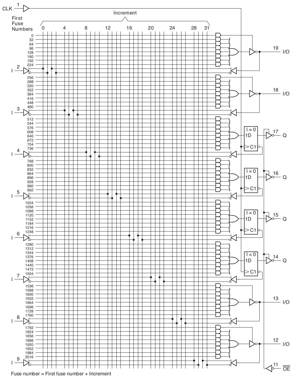
The layout and pinout of the PAL can be seen below, where the inputs assigned as follows:
- !reset - (pin 2) Reset (active low)
- pclk - (pint 3) processor clock
- hblank - (pin 4) horizontal blank (active high)
- DD7 - (pin 5) sign bit of accumulator (1 = negative, 0 = zero, or positive)
- I4..7 - (pin 6..9) high nibble of lower instruction register
![]()
The exact logic functions can be seen in the GitHub repo. The compiled version is shown below as a 2048-bit mask where each zero represents a connection in the grid above.
                   11110111111111111111111011111111
                   11110111111111111111011101111011
                   11110111111111111111111110110111
                   11111111111111111111111111111111
                   11111111111111111111111111111111
                   11111111111111111111111111111111
                   11111111111111111111111111111111
                   11111111111111111111111111111111
                   11110111111111111110111111111111
                   11110111111111111111111111110111
                   11110111111111111111111101111111
                   11110111111111111111011111111111
                   11111011011111111111111111111111
                   11111111111111111111111111111111
                   11111111111111111111111111111111
                   11111111111111111111111111111111
                   11111111111001111111110111111011
                   11111111110111111111111011111111
                   11111111110101111111111111111111
                   11111111110111111111111110110111
                   11111111111001111111110101111111
                   11111111111111111111111111111111
                   11111111111111111111111111111111
                   11111111111111111111111111111111
                   10111111111111111111111111111111
                   01111111111111011111111101111111
                   01111111111111011011111111111111
                   01111111111111011111111011111111
                   01111111111111011111101111111111
                   01111111111111011111111111111011
                   11111111111111111111111111111111
                   11111111111111111111111111111111
                   01111111111111111110111010111111
                   11111111111111111101111011111011
                   11111111111111111111111111111111
                   11111111111111111111111111111111
                   11111111111111111111111111111111
                   11111111111111111111111111111111
                   11111111111111111111111111111111
                   11111111111111111111111111111111
                   11111111111111111110100110111011
                   01111111111011111001011011110111
                   01111111110111110101111011110111
                   01111111111111110101101011110111
                   01111111111111111101111001110111
                   11111111111111111110111001111111
                   01111111111111111110111010111111
                   11111111111111111111111111111111
                   11111111111111111111111011111111
                   11111111111111111111111110110111
                   11111111111111111111111111111111
                   11111111111111111111111111111111
                   11111111111111111111111111111111
                   11111111111111111111111111111111
                   11111111111111111111111111111111
                   11111111111111111111111111111111
                   11110111111111111111111110110111
                   11110111111111111111111011111111
                   11111111110111111011011110110111
                   11111111111011110111011110110111
                   11111111111111111111111111111111
                   11111111111111111111111111111111
                   11111111111111111111111111111111
                   11111111111111111111111111111111
The original PAL16R4 is no longer available, but there is a modern equivalent in the ATF16V8B. This is a GAL (generic array logic) which can be programmed to resemble a variety of PAL devices including the PAL16R4. The GAL contains 250 gates, but only 80 of these are used as follows:
- 32 AND gates
- 8 OR gates
- 4 registers (10 gates each)
-
Scan Lines and Flicker
08/13/2019 at 03:38 • 0 commentsVideo testing would never be complete until a CRT was put into the mix. This whole exercise started with the assumption that LCDs would handle arbitrary video timing. How hard is it to do a simple linear interpolation and resample at the native resolution of the LCD display? Too hard apparently, or at least no one wanted to deal the potential Nyquist-gone-bad corner case.
Luckily my custom modes are close enough to existing standards to be supported by most reasonable LCD monitors. Older HD or newer UHD TVs not so much, but there is a relatively inexpensive converter box to cover these as well.
It still left a gap though. There once was multi-sync magic where no one cared what resolution you wanted. You just generated as many or as few lines as you wanted. Just pick two frequencies for H and V and bingo, the mode would just work. Were CRTs just a myth?
![]()
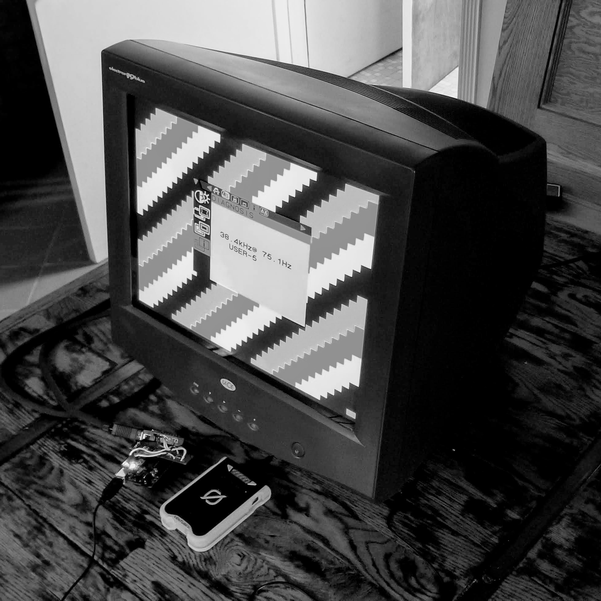
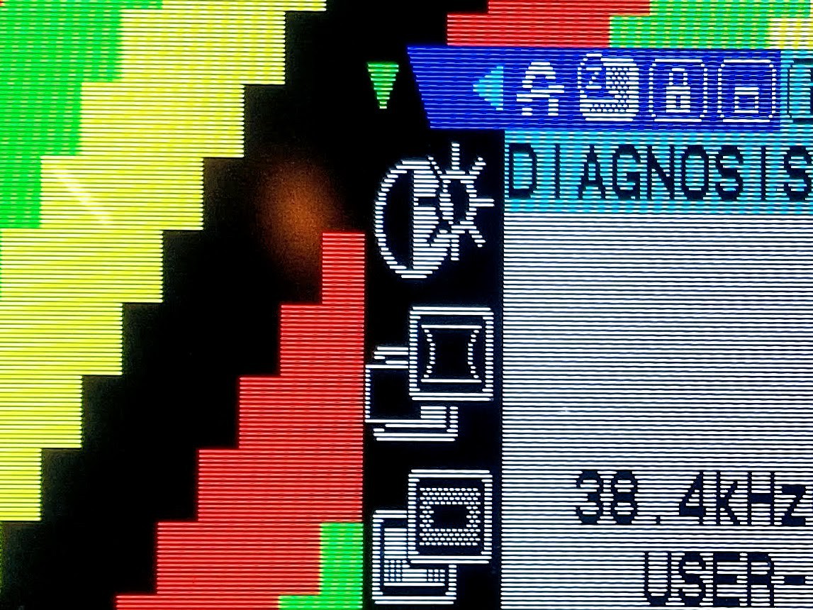
My last CRT monitor was jettisoned over a decade ago, so the hunt was on. I was able to find a retired graphics designer who was downsizing and letting go of a LaCie electron 19blue. This circa-2001 display uses a Mitsubishi Diamondtron CRT and supports a horizontal frequency range of 29-110 kHz, a vertical range of 49-140 Hz, and has a video bandwidth of at least 200 MHz.
These specs are way beyond my requirements, so no issues handling whatever I can throw at it. The example below is the 38.4 kHz horizontal timing, but with a vertical timing of 120 Hz. The result is a 300-line display that shows off the scan lines nicely.
![]()
120 Hz looks great, but going the other way exposes one long forgotten side-effect of CRTs: Flicker. The advantage, and in some cases disadvantage, of LCDs is the relatively long persistence of the image. CRT phosphors have almost no persistence and they rely on the brain's persistence of vision. The SVGA 60 Hz mode looked fine on the LCD but was almost painful to watch on the CRT.
The VGA 75 Hz mode is a lot more tolerable and would definitely be the preferred choice for any text modes when displayed on a CRT. However, I'm leaning towards supporting both VGA and SVGA for all graphics modes. The 60 Hz SVGA provides the most lines of text for an LCD. If refresh is an issue then the 75 Hz VGA is available at the expense of just a few lines of text.
-
More Video Testing
08/10/2019 at 04:12 • 2 commentsThe net was cast wide to capture additional problematic video displays. This chance discovery was abandoned by the side of the road, probably because the main digital board was faulty and the owner didn't want to pay to dispose of it correctly. The panel was still good even though it had survived at least one rain storm. Replacement parts are readily available on Ebay and the repair was made.
![]()
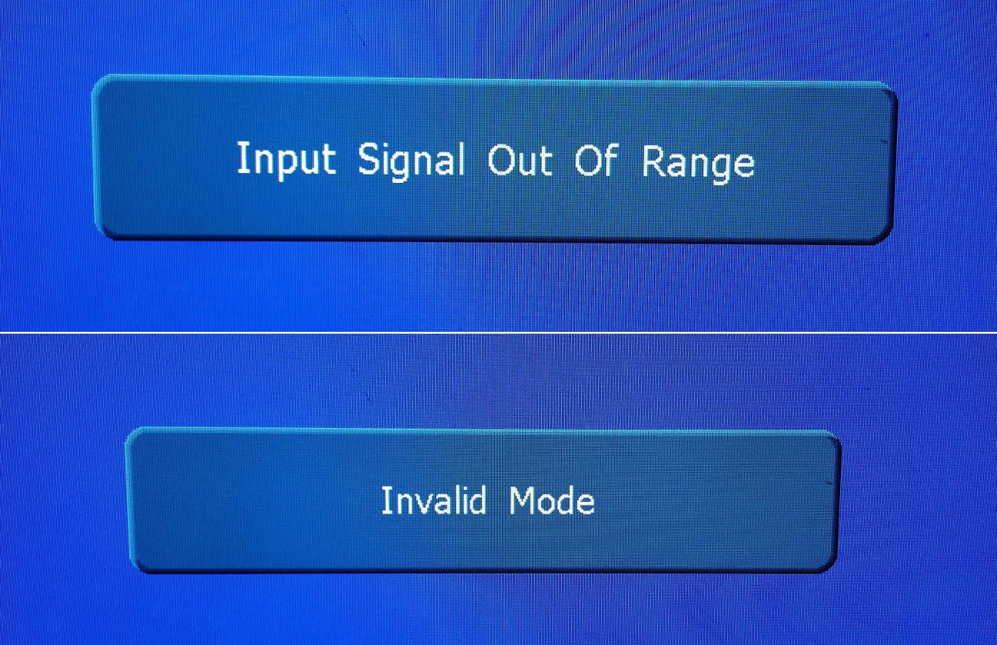
The result was a working 720p plasma TV from 2006 with both VGA and an original HDMI 1.0 input. It proved to be the most problematic of all displays so far. Not only was the 38.4 kHz horizontal scan frequency rejected (invalid input) but it could not accept a valid signal with a vertical frequency above 60 Hz (out of range).
![]()
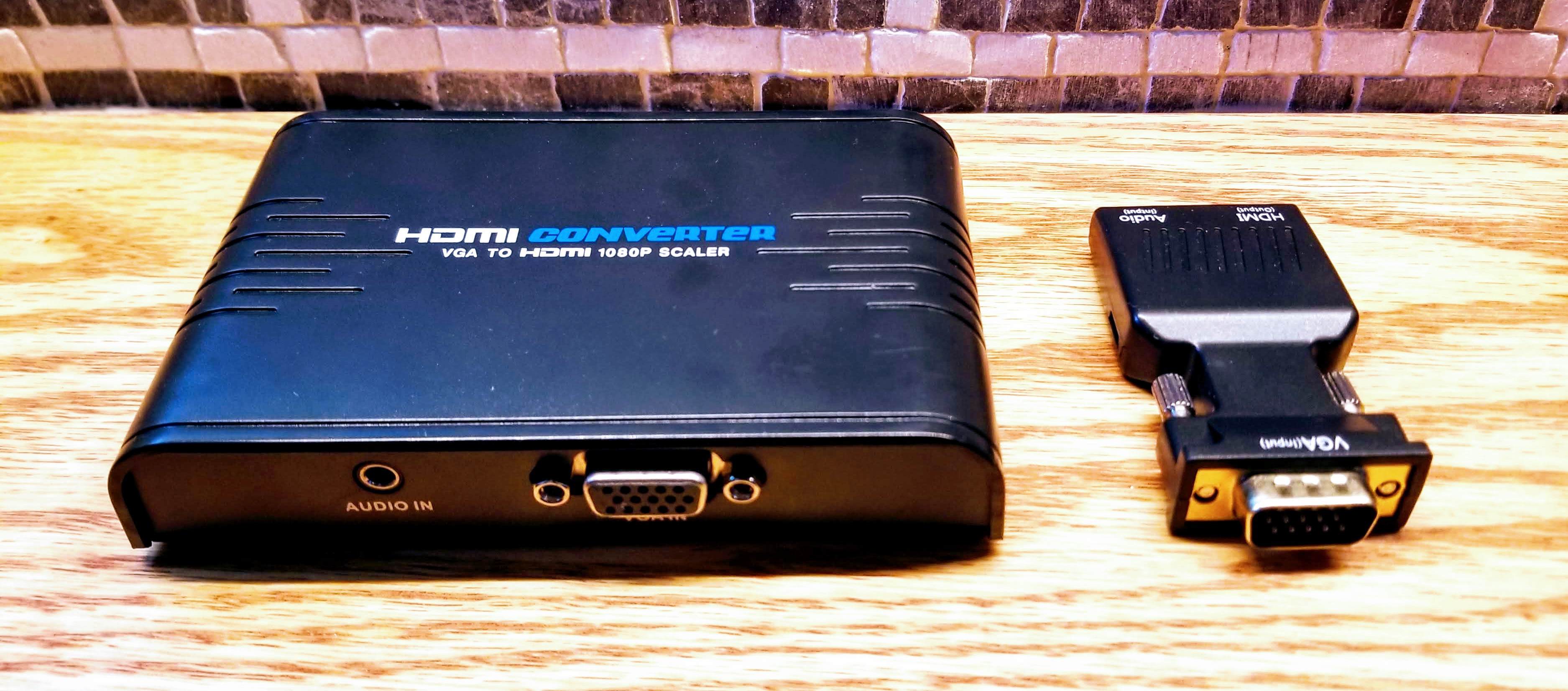
Meanwhile I ordered a VGA to HDMI converter/scaler. This is the more powerful and expensive option at $16 vs $7. This device (on the left) consumes the VGA signal and regenerates it at a selectable 720p or 1080p from the HDMI output. The cheaper version (on the right) just passes the signal through, converting the analog VGA to a digital HDMI signal with the original timing and resolution intact.
![]()
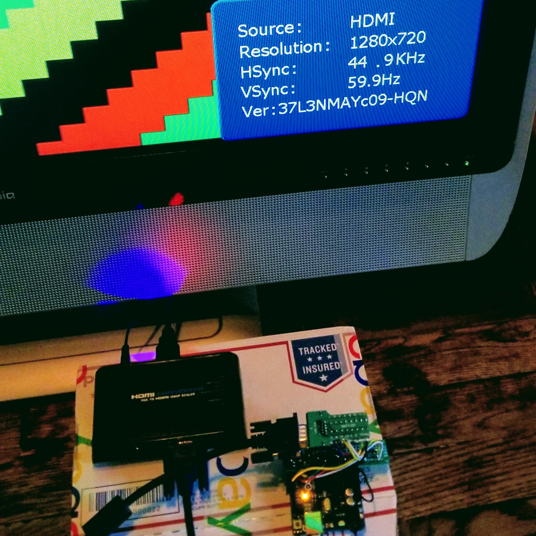
This scaler had no problems with the 38.4 kHz horizontal and 75 Hz vertical timing. It can output the 720p HDMI signal at 60 Hz that the ancient recycled TV can accept. Not only that, it can output 1080p and provide a way to display 640x480 on the very latest UHD TV.
![]()
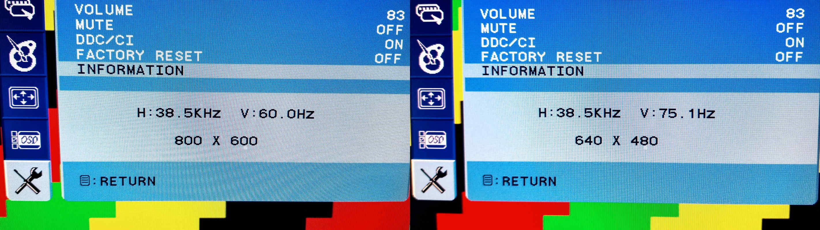
So this provides an inexpensive get-out-of-jail-free option for displays that can't handle the 38.4 kHz and/or 75 Hz frequencies. This has only been an issue with older TVs though (pre-2010). All the computer monitors tested so far seem to be OK with the timing. They do have limitations, but sending an extra 12 lines per field is not causing problems.
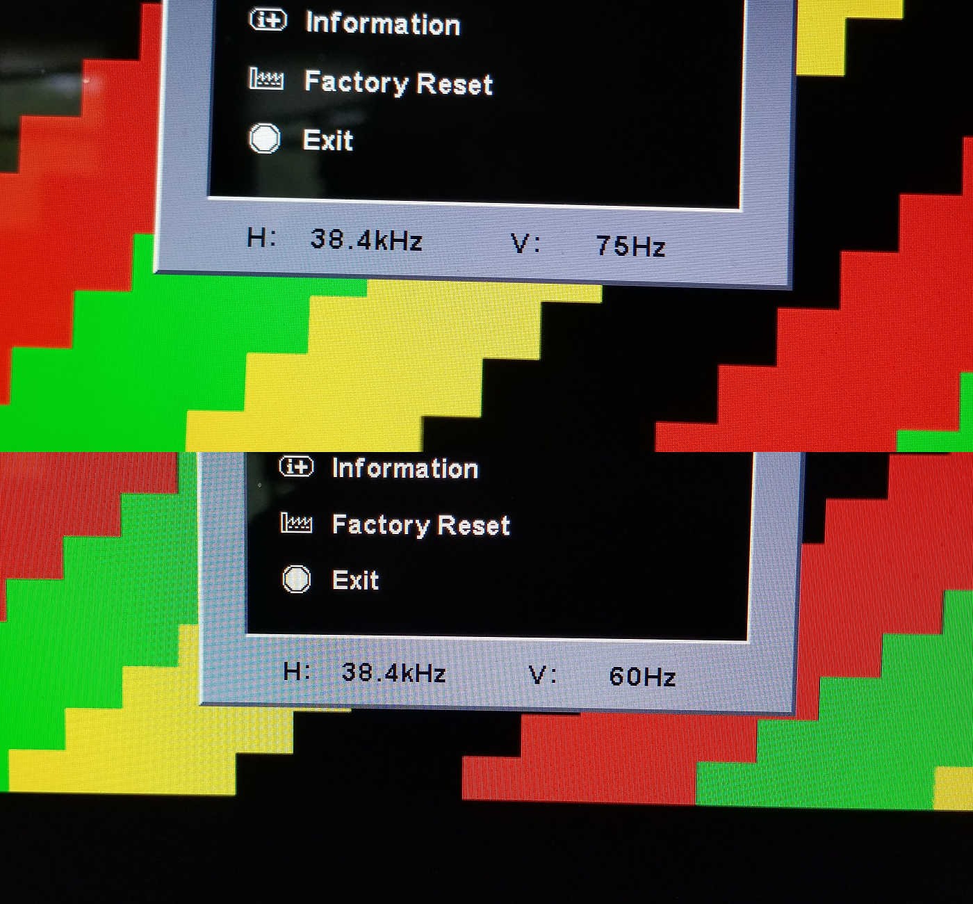
Shown below is a monitor that displays 640x480 or 800x600 when given the correct timings. It will switch to display the H and V frequencies when given the non-standard timing, but still displays it correctly at those resolutions.
![]()
Now all the bases are covered on the display front the current design can continue.
-
Video Testing
08/05/2019 at 03:14 • 1 commentThings inevitably slow down during the summer. Not much happened in July and it will probably stay that way until well in to September. The project is still active though and the plan is to get a working PCB built by year end.
The last two logs detailed some significant design changes. The GPU change is based on the assumption that both the horizontal scan and serial communication timing can be combined. The only frequency where this is possible is 38.4 kHz. Unfortunately, there are no defined video modes that use this frequency. The hope is that monitors will support some form of generalized timing.
You would think a simple Google search would yield some answers to this question, but alas no. There is a standards body that was formed to define this stuff, the Video Electronics Standards Association (VESA). They created four standards of interest:
- Display Monitor Timing (DMT)
- Generalized Timing Formula (GTF)
- Coordinated Video Timings (CVT)
- EDID Timing - defined by the Extended Display Identification Data (EDID)
The first document detailed a set of standard video modes. But this was during the era of multisync and multscan montors that could support an arbitrary range of video timings. So how arbitrary? VESA came up with the GTF to define these generalized timings. But they were too general and no one could support them. Then came CVT to put some constraints on things as well as introduce reduced blanking. Both GTF and CVT define generalized video timing that would support a video mode of interest.
So do monitors support these generalized standards? Apparently not. The final standard (EDID) provides a way for the monitor to tell the graphics card that is does not support generalized timing and list the few standard timings it does. This appears to be how everything works these days and only defined standard video modes are available unless you can dig up a 20-year old multisync CRT monitor.
So how standard does standard have to be? There are a couple of standard video modes that come close:
- 640 x 480 - 75 Hz vertical, 37.5 kHz horizontal, 31.5 MHz pixel frequency
- 800 x 600 - 60 Hz vertical, 37.9 kHz horizontal, 40 MHz pixel frequency
The ability to generate a usable video signal is a gating factor for the continuation of the new design, so this needs to be tested. This was a blocker so it was time to do some experimentation. This was done by modifying Nick Gammon's Arduino sketch to generate a VGA signal. The timer settings were changed to generate the 38.4 kHz horizontal frequency and both the 60 or 75 Hz modes were tested.
The results were slightly mixed, but promising. Two older LCD TVs had very little tolerance for non-standard timings and would not sync. Newer LCD monitors and TVs had no trouble handling the higher frequency as can be seen below.
![]()
[Note: the timing is slightly fast and the numbers are rounded up in the above images]
The acid test was to see if a cheap VGA to HDMI converter could handle this timing. This is important since VGA support is in terminal decline. Almost no monitors and TVs now ship with a VGA input, so a VGA to HDMI converter may be required as part of the standard configuration.
[Update] After additional testing it appears the cheaper VGA to HDMI converters are just simple analog-to-digital converters with a buffer and data serializer. This means what ever frequency you give them is just passed through from the VGA input to the HDMI output. The hope was a device like this would convert the non-standard timing and support the more sensitive monitors. Additional testing confirmed that if the monitor does not support the non-standard timing via the VGA input then is will not accept the timing via the HDMI converter.
A panacea to this timing issue may still be available in the form of a VGA to HDMI converter/scaler. This is a more expensive device, but will actually consume the VGA input signal and then generate a 720p or 1080p HDMI signal. This will provide a stable and usable signal assuming the scaler accepts the non-standard VGA input timing. This also solves another potential issue: The latest UHD TVs no longer support 480p and won't accept 640x480 even with the correct timing!
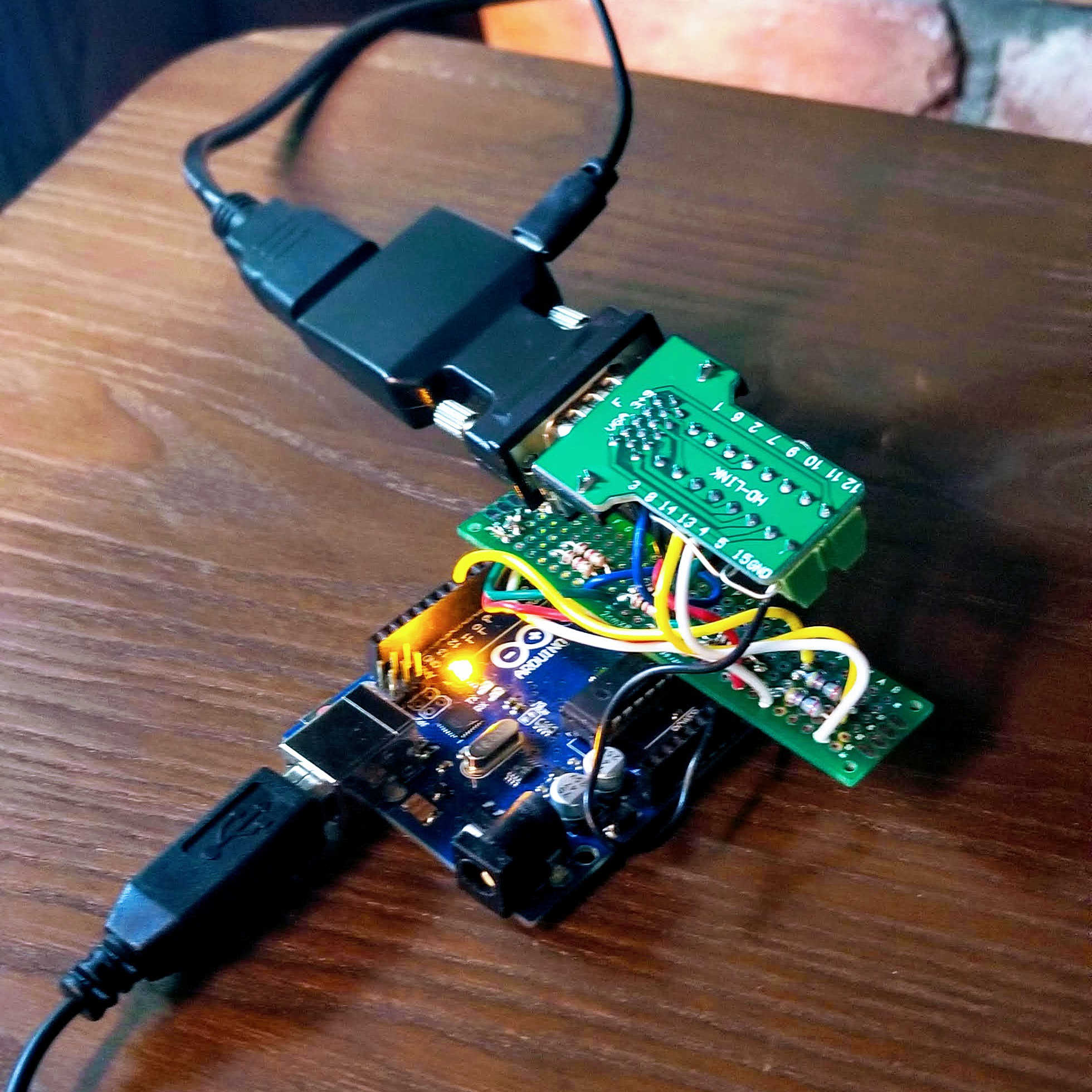
The picture below shows the Arduino, VGA breakout, and a cheap $7 VGA to HDMI converter.
![]()
So to wrap up, here are the details of the planned video modes: The pixel/dot clock will be 31.95 MHz (although 32 MHz is close enough). This is divided by 4 to generate the process clock to drive the horizontal counter. The counter starts at 32 and counts to 240, for a total of 208 process cycles or a frequency of 38401.44 Hz.
The text mode and hi-res graphics mode will use a vertical frequency of 75 Hz. This requires a total of 512 lines to divide the 38.4 kHz down to 75 Hz. The true standard uses 500 lines to divide down a 37.5 kHz horizontal frequency. This means sending an additional 12 lines per field.
The lo-res graphics mode will use a vertical frequency of 60 Hz. This requires a total of 640 lines to divide the 38.4 kHz down to 60 Hz. The true standard uses 628 lines to divide down a 37.879 kHz horizontal frequency, again an additional 12 lines will be sent. The low-res pixels are sent at a rate of 8 MHz while the monitor samples with a 40 MHz dot clock. This means each pixel is stretched to 5 on the SVGA display, so each line will be repeated 5 times to match.
-
16-bit Instructions
06/24/2019 at 05:16 • 0 commentsThe redesign continued to ECU section. The changes are fairly significant, so much so that the breadboard build needs to start over. It was almost back to the drawing board, but the CPU section remains fairly intact. The result is another reduction in chip count to bring the TTL count down to 37 chips.
The original design packed the instructions into just 8-bits. The instructions need to define the instruction type, ALU function, data source, and destination register. The original encoding resulted in a lot of limitations in the available instructions to pack so much into so little space.
The instructions do provide everything needed to write code, but actual programs were quickly exposing the instruction set limitations. Quite often additional instructions are needed to move the result from the ALU to the desired register. There is no specific move instruction, so this requires the ALU identity function to target the final register. This results in a lot of wasted cycles.
The solution is to expand the size of the instructions. The ROM is still 8-bits wide, so this requires an additional cycle to load another byte to get to 16 bits. However, one bit of the first instruction byte can be used to tell the state machine if a second instruction byte should be loaded. This allows variable-length instructions, with a limited set of 7-bit instructions and a full set of 16-bit instructions.
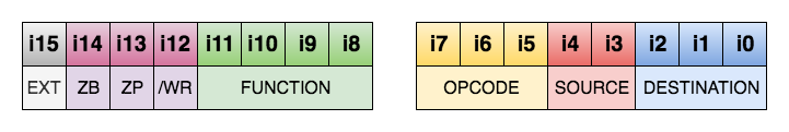
The new design is using instructions of this format:
![]()
Destination is one of the 8 possible registers (Pg, PC, SC, V, HL, E, X, Y). Source is one of 4 data sources (A, X, E, RAM). There are 8 possible opcodes, with the following 6 defined:
- LD - load operand (source not used)
- LDC - load conditional (source defines condition)
- MV - move source to destination
- FNH - ALU unary function defined by H - destination = FNH(source)
- FN4 - nibble-wide ALU binary function
- FN8 - byte-wide ALU binary function
The first 4 opcodes define 7-bit instructions. The most-significant bit of these is high and this stops the state machine from loading the second byte. The most-significant bit is also the output enable (active low) of the second instruction register, so the second register is tri-stated and the value pulled high to 0xFF. The ALU binary functions require all 16-bits, so the most-significant bit of the last two opcodes is low. Along with the 4-bit ALU function there are some additional bits as follows:
The /WE bit (active low) enables write enable on the RAM cycle and stores the result in memory. The ZP bit (active high) specifies the zero page when the RAM is addressed. In a similar way, the ZB bit (active high) specifies the zero bank (the memory bank that contains the display). The EXT bit (active low) specified a set of extended registers and will switch the destination from the internal 8 registers to 8 possible external registers.
The default values of the second instruction byte are therefore: internal registers, zero bank and page, memory read only, FNH ALU function. This means the RAM source comes from the zero page in the zero bank for the 7-bit instructions.
This instruction format now defines almost everything needed in a single instruction. This improves performance, even though some instructions require an additional cycle to load the second instruction byte. The new format is using about 60% of the cycles to run the same code. The simpler encoding also reduces the amount of logic in the ECU, so a net reduction in chips, even though a second instruction register was added.
Next up is a new schematic, complete redesign the PAL, and redo the entire breadboard... so basically, back to square one :(
-
Yet Another Redesign
06/20/2019 at 02:34 • 0 commentsIn keeping with a lot of the previous logs, the recent GPU writeup is now obsolete. As predicted, better insight gained through the software design is driving hardware changes. In this case the GPU can be simplified by moving the slower counters to software.
The original GPU design takes care of almost all video timing, so the CPU interpreter loop can synchronize with a standard baud rate. If the baud rate can be aligned with the display then the same timing overhead can be used for both serial and video. This can be achieved by using a horizontal scan frequency of 38.4 kHz and a baud rate of 38400 (or dividing down to 19200, 9600, etc).
Running the VESA GTF against this for a standard vertical frequency gives the following mode line:
# 640x490 @ 75.00 Hz (GTF) hsync: 38.40 kHz; pclk: 31.95 MHz
Modeline "640x490_75.00"  31.95  640 672 736 832  490 491 494 512  -HSync +Vsync
The exact dot clock is 31.9488 MHz and this is available in a 31.95 MHz crystal. The mode defines 490 lines, but only 480 would be displayed with 5 additional vertical blanking lines at the top and bottom of the screen.
With this change both the scan and vertical counters can be eliminated and replaced with registers that are updated every horizontal scan. An additional chip of gates is also eliminated to reduce the design by a total of 4 chips.
-
ROM
06/17/2019 at 03:37 • 0 commentsFocus shifted to building the ROM this weekend. Here's a quick overview of the contents:
- Native Program (128k) - code executed natively by machine.
- ALU (56k) - lookup tables containing ALU results.
- Relocatable Code (40k) - code executed by interpreter.
- Fonts (32k) - binary fonts used in text mode and dithering patterns used in hi-res graphics mode.
The machine uses an 8-bit program counter (PC) and 8-bit page register (Pg). An additional bit of state (bank) is held by the CPU state machine to define two banks of 64k, providing the 128k of address space.
The upper 128k contains various lookup tables. These can be split into two general sections: 96k of ALU functions and 32k of fonts. The ALU contains 56k of math and logic functions, including four 8-bit wide binary functions (ADD, SUB, AND, OR), three 4-bit wide binary functions (MUL, DIV, MOD), and 48 unary functions (discussed in earlier logs).
The remaining 40k of ALU functions are reserved for relocatable code. These act like the other functions but return a byte of code as the result of the function. This may sound odd, but it is the most efficient method of reading data from the ROM using the Harvard Architecture. The alternative is to write a program that would load a the byte of code as an operand, write it to the RAM, then increment a pointer to the next memory location. It would take at least 3 bytes of native code to write each operand to memory, requiring almost all 128k of program memory to load 40k of interpreted code.
The final part of the ROM are the fonts. There are two sets of four fonts. The first set use 8x8 glyphs and the second use 8x16 glyphs. The initial plan was to have bold and italic fonts, but this really isn't possible at 8-pixels wide! There are some other options though and these can be broken down as follows:
- Thick Serif
- Thin Serif
- Thick San-serif
- Thin San-serif
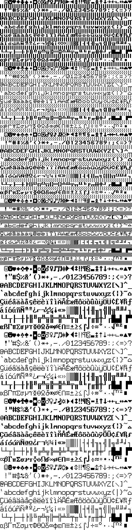
Two sets of these fonts were selected from The Ultimate Oldschool PC Font Pack. It was quite challenging to process the old bitmap files, but this excellent resource was able to pull out the data and even render it as simple text files. From there a script packs the fonts into the 32k font area of the ROM. A test script was used to verify the ROM and generate the following PNG:
![]()
All the fonts can be seen one after another. The first 4 fonts only take up 8 lines and the other 8 lines are used for dithering patterns in the hi-res graphics mode (discussed in the last log).
-
GPU - part 2
06/12/2019 at 15:49 • 0 commentsThe GPU uses three 4-bit counters (scan counter and V register) to control the vertical resolution of the display. This combined 12 bits can render up to 4096 vertical lines. Only part of this range can be displayed at standard video refresh rates using the 30.875 MHz dot clock though. The display is limited to 512 lines at 60 Hz or 400 lines at 75 Hz. Overclocking allows more lines with the potential for 1024 lines using a 64 MHz dot clock.
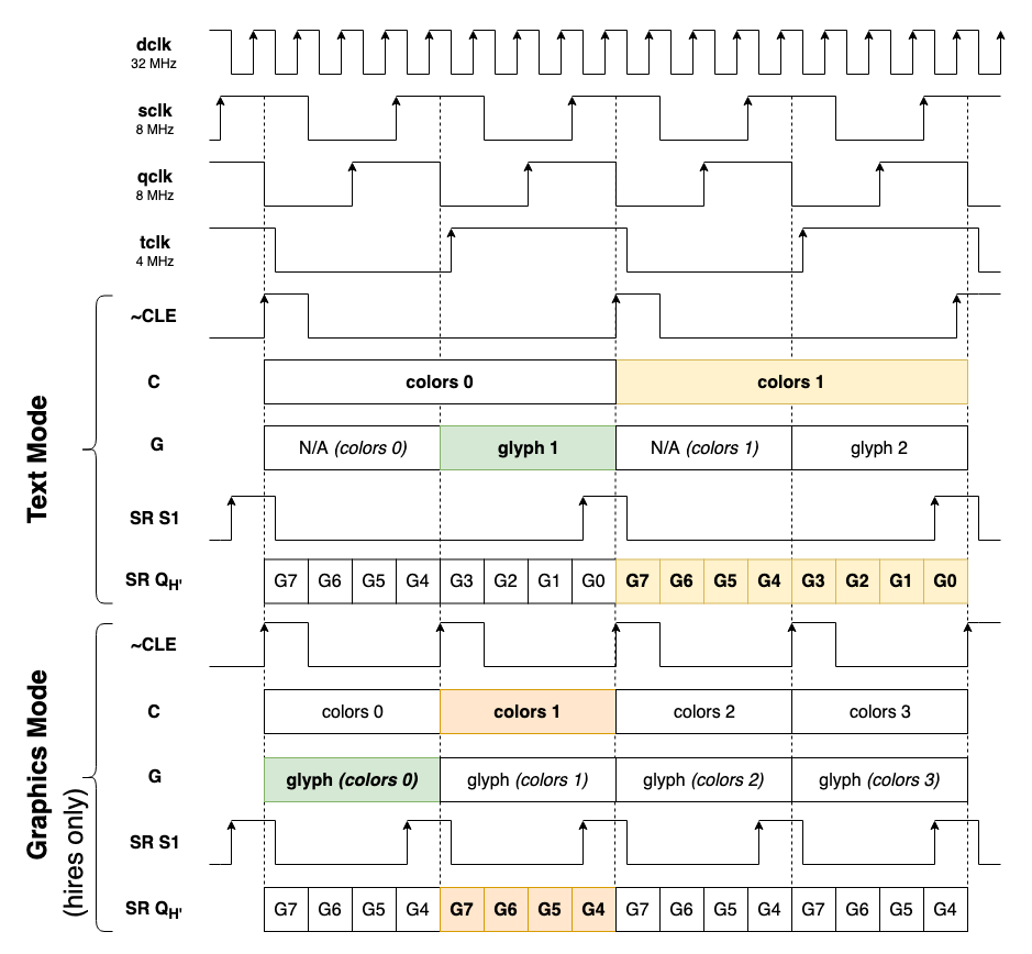
As well as the counters, he GPU uses two additional registers: The Color Register (C) and Glyph Register (G). The C register stores the current color(s) being displayed and can be used in two ways: It can represent a single 8-bit color as a 3:3:2 RGB value, or two 3-bit RGB colors and a 2-bit font value. Note: The pipeline timing dictates this 2-bit value will select the font of the next character.
The G register acts as a pipeline to hold the next glyph pattern while the current one is being rendered. The value of the G register is loaded into a shift register (SR) that is clocked at the 32 MHz dot clock. The output of this shift register is used to select one of the two 3-bit colors stored in the C register. The C register and this multiplexer can be thought of as an extremely simple RAMDAC.
In text mode the GPU uses two process cycles per character: The first to load the G register and the second to load the C register. Both must be synchronized so the shift register load happens at the same time as the C register load. The exact timing is shown in the diagram below.
![]()
The GPU repeats the same line from the video memory either 8 times in hi-res text mode, or 16 times in lo-res text mode. The scan counter counts to either 8 or 16 to select the specific line from the font ROM to render for the character's glyph.
The hi-res graphics mode uses all the same logic as the text mode, but operates on a single process cycle. The C and G/SR load signals now happen at the same time, so the same byte is loaded by the C register and passed though the font ROM to load the G register.
The GPU reads the same line only twice in the hi-res graphics mode and the shift register will output only 4 bits before the next value is loaded. The rendered character is therefore 4x2 pixels rather than the hi-res 8x8 or lo-res 8x16 text mode characters. This mode uses a special font where all the characters have the same glyph. There are still 4 fonts available though, since only 6 bits are used for the two colors.
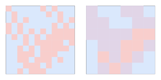
The first font (dither 0) consist of a 2x2 block of foreground pixels followed by a 2x2 block of background pixels. The other 3 fonts provide dithering patterns that blend the two colors to provide a wider pseudo palette of up to 32 colors. The patterns also alternate on odd/even lines as shown below repeated 4 times.
![]()
The example below shows how the dithering (on the left) is used to represent an intermediate color (shown on the right). Note: The hi-res graphics mode defines a typical resolution of 320x240 pixels, but the dithering is rendered at the native 640x480 resolution.
![]()
Finally, in lo-res graphics mode all the glyph logic is bypassed and the C register is treated as a single 8-bit color value via its own video DAC. The GPU reads the same line four or five times to define a resolution of 160x120 with a simple one-byte-one-pixel format. Only half the video memory is used for one screen in this mode, so it provides room for double buffering. This is essential to prevent flicker when updating sprites on the screen, making it the preferred video mode for retro games.
-
GPU - part 1
06/09/2019 at 01:21 • 0 commentsThe GPU consists of five 74F163 4-bit synchronous counters. The system is fully synchronous, so all counter receive the same 7.72 MHz clock regardless of the rate at which they ultimately count. The count is controlled by cascading the RCO/ENT (TC/CET) signals between the counters.
The first two counters form the Horizontal (H) register and connects to the lower half of the RAM address bus. The RCO signal from the second counter of the H register is used to reload the lower counter with a value of 12. This creates a count cycle that rolls over to 12 rather than 0 for a total count sequence of 244.
The H register is used to generate the horizontal timing signals and these are based on the VESA display timing formula (DTF). Generally this specifies a horizontal blanking (H-blank) period of 20% (48.8 cycles) and a horizontal sync (H-sync) period of 8% (19.52 cycles).
The H-sync is active when the upper 3 bits of the H register are low, so when the count is less than 32. Since the count starts at 12 the H-sync period lasts for 20 cycles, or 8.2% of the horizontal scan. The H-blank is active when the upper 2 bits of the H register are low and the next most significant 3 bits are not all high. This is the case when the count is less than 56 (64 - 8). Again, since the count starts at 12, this actually translates to 44 cycles. The RCO signal is also added the H-blank period, so the total blanking period is 45 cycles. This is slightly short to allow two cycles of overscan at the start and end of the blanking period to reach the required 49 cycles, or 20.08% of the horizontal scan.
The H-blank signal is used to inhibit the video DAC switch and effectively turn off the video signal for the 45 cycles of the blanking period. The video signal will be output for the other 199 cycles, where at least 4 of these cycles are still in the DTF blanking period. The nominal width of the display is 192, so the first 4 and last 3 cycles are considered to be overscan and would typically be blank pixels. However, the option exists to shift the screen slightly to the left or right to accommodate different monitors.
The RCO signal of the H register is used to enable the clock of the Scan Counter (SC). This is a single 4-bit counter that can count up to 16 horizontal lines. The outputs of the SC are combined, typically with AND gates, to create four additional RCO signals. These signals go high when the count reaches 1, 3, 7, or 15. The first of these signals is just the lower bit of scan counter and the last signal is the actual RCO of the counter.
These RCO signals allow the next counter to clock on every 2, 4, 8, or 16 horizontal lines. The specific signal depends on the video mode selected and will be described in details in the next log. The selected signal is used to enable the clock of the remaining two counters that form the Vertical (V) register. This register connects to the upper half of the RAM address bus allowing the combined H and V registers access to 61k of RAM (remember, the H register starts at 12).
The vertical count does not reset and will continue until it wraps around and returns to zero. The vertical register is accessible to the CPU though as one of it's 8 register targets. It is the responsibility of the CPU to reload the V register at the vertical scan rate of the video display. The CPU is also responsible for generating the vertical blank and sync signals by setting the appropriate bits on the extended (E) register.
Novasaur CP/M TTL Retrocomputer
Retrocomputer built from TTL logic running CP/M with no CPU or ALU