Alastair Hewitt
-
Clocks, Scans, and Refresh Rates
04/10/2019 at 22:22 • 0 commentsThe previous log discussed the display columns. This one will cover the rows, but first the clocks:
- Dot Clock (dclk) - 25.175 MHz
- Machine Clock (mclk) - 12.588 MHz (1/2 dclk)
- Processor Clocks (pclk/qclk) - 6.294 MHz (1/2 mclk, qclk is pclk inverted)
- Extended Clocks (rclk/sclk) - 6.294 MHz (pclk/qclk shifted 90-degrees)
- Text Clock (tclk) - 3.147 MHz (1/2 pclk)
The dclk is the standard VGA dot clock and is used to latch the output of the first video DAC (VDAC1) and to shift the bits of the character buffer in text mode. This renders the text at the full 640 horizontal graphics resolution of VGA by displaying 80 columns of text using 8-bit wide characters (not the 9-bits of the 720 horizontal resolution VGA-400 text mode).
The mclk is the native speed at which the hardware is clocked at. This is divided down again to generate the pclk at which each processor operates. Therefore each processor cycle includes two machine cycles. One machine cycle is used to access the ROM and the other to access the RAM. The GPU and CPU operate on opposite clocks to access both memories concurrently.
The rclk is a delayed version of the pclk used by the CPU state machine. This provides a 40ns delay in which to perform the instruction decode and maintain the state across the edge of the 80ns machine cycle.
The final clock is the tclk and is used by the GPU in text mode. Each column of text uses two bytes, so the GPU divides down the pclk to alternated between reading the ASCII code point and font/color bytes on each processor cycle.
Each line of the display requires 200 process cycles as discussed in the previous log. This results in a horizontal scan frequency of 31.47 kHz. This is fixed in hardware and is the same for every video mode. At the end of each line the Scan Counter (SC) is incremented. This is a 4-bit counter that can count up to 16 lines. This serves two purposes:
- Index the character bitmap row to be rendered in text mode
- divide down the line count
The lo-res text mode uses 16 lines for each character, so the whole of the scan counter is required for this. The hi-res text only needs 8 lines, so just the first 3 bits are used. The bits are also combined to create an ent signal for the vertical counter depending on the video mode as follows:
- divide by 2 - hi-res graphics mode (repeat lines twice)
- divide by 4 - lo-res graphics mode (repeat lines 4-times)
- divide by 8 - hi-res text mode (8-bit character)
- divide by 16 - lo-res text mode (16-bit character)
This is what drives the vertical scan count, but the software must blank the display at the bottom of the screen, generate the V-Sync pulse, and then reload the V register to reset the counter to the top of the screen. The value loaded in to the V register can be moved up and down to perform a smooth scroll of a larger text area within the video RAM.
Since the vertical sync timing is software defined it is possible to supported different screen sizes. The YATAC defines 4 screen heights and when combined with the 4 other video modes provide a total of 16 configurations for the display. Both the standard VGA-400 and VGA-480 modes are supported, allowing full compatibility with even the most ancient PS/2 CRT monitors. The other two modes are YATAC-specific custom defined: The YATAC-9x4 is a 419 line mode at 75 Hz and will map directly to HD/UHD 9:4 ratio displays (but at a much lower resolution). The YATAC-MAX is a 561 line mode at 56 Hz and renders the maximum number of lines in RAM (256) when using the hi-res graphics mode.
The mode name, total lines and how they are made up are defined as follows:
Mode Name Total Lines Front Porch V-Sync Back Porch Refresh Rate YATAC-9x4 419 17 2 40 75.10 Hz VGA-400 449 12 2 35 70.09 Hz VGA-480 525 10 2 33 59.94 Hz YATAC-MAX 561 12 2 35 56.09 Hz The screen refresh rate drops as the lines increase since the horizontal frequency is fixed. However, even the custom modes are designed to fall in line with standard refresh rates that most monitors should support. All 16 modes are shown below along with the line count for each:
Refresh Rate
Native VGA
Hi-Res Graphics
Lo-Res Graphics
Hi-Res Text
Lo-Res Text
75 Hz 360 180 90 45 22 70 Hz 400 200 100 50 25 60 Hz 480 240 120 60 30 56 Hz 512 256 128 64 32 Finally there is the RS232 serial communications. The plan is to support multiple baud rates up to 38400 baud. The highest speed would require processing one bit every 164 machine cycles and a whole byte would take 1476 machine cycles to transmit/receive. This seems achievable, but that speed might be dropped once development reaches that stage. The era-appropriate rate would be 300 baud, but I'm hoping to do better than that.
-
Counting to 200
04/10/2019 at 18:16 • 0 commentsThe GPU does the same thing over and over again: Count to 200. It does this regardless of the graphics mode. Each horizontal scan will read 200 bytes of the RAM at the processor clock rate of 6.25 MHz. What does change is what each byte represents.
Even though the horizontal scan is 200 bytes long, it must also contain the border, overscan area, and sync timing. This extra stuff takes up 20% of the scan line, so only 160 bytes are typically displayed per line.
The 160 bytes is mapped to columns as follows:
Mode Bits per Column Columns Hi-Res Graphics 4 320 Lo-Res Graphics 8 160 Text 16 80 Each column in the graphics mode is directly mapped to a DAC. The hi-res 4-bit encoding is RGBI and the lo-res 8-bit encoding is RGB 3:3:2 (3-bits red and green, 2-bits blue). The text column contains two colors (foreground and background) and both use a 3-bit encoding of just RGB.
The 16 bits of a text column span 3 bytes and consists of the font, code point of the character, and two colors. The following table shows how these are mapped given a column index of C:
Byte[C-1] Byte[C] Byte[C+1] Font 2 bits Code Point (ASCII) 8 bits Foreground Color 3 bits Background Color 3 bits In addition to the 160 bytes per line for the conventional display area, an additional 4 bytes are added to the start and end of each line. These bytes would normally be set to a solid border color and are rendered along with the normal 160 bytes. These can be used to display content in the border, but this would only be visible on a CRT and wrap around the edge of the glass.
The display RAM provides up to 256 rows for the display. The total RAM required is 42k bytes with the 168 bytes reserved for each line for the display. The way this is mapped may seem a bit odd until you see the reasoning behind it.
The first column of the display (including the border) has an index of 56 (0x38 in hex). Remember we need to count to 200. A naive approach would be to start at 0 and count to 199 before returning to zero on the next clock pulse. If we start at 56 then the last index before reseting would be 255. The synchronous counter chips provide a signal (rco) that is generated on 255 and this can be used to reload the counter to 56. Therefore we count to 200, but without needing any additional logic gates (actually, one inverter)
So why place the border where it is? And why is it the size it is? The (VESA) VGA spec does specify a border, but this would only be 2 bytes (8 VGA pixels). The extra 2 bytes is added so the screen border ends at 224 (0xE0). This is when the H-Sync pulse begins. A single 3-input AND gate can be used to define the start of this pulse. This is the H-Blank signal and defines when the horizontal output should be turned off. The H-sync pulse lasts for 24 bytes, so a pair of 2-input NAND gates can fully define this when combined with the H-Blank signal.
Here's the detailed memory map of a line of video RAM:
Binary Hex Decimal Description 0011 1000 0x38 56 video RAM start 0011 1001 0x39 57 back porch end 0011 1010 0x3A 58 left border start 0011 1011 0x3B 59 left border end 0011 1100 0x3C 60 display start 1101 1011 0xDB 219 display end 1101 1100 0xDC 220 right border start 1101 1101 0xDD 221 right border end 1101 1110 0xDE 222 front porch start 1101 1111 0xDF 223 front porch & video RAM end 1110 0000 0xE0 224 H-Blank & H-Sync start 1111 0111 0xF7 247 H-Sync end 1111 1000 0xF8 248 back porch start 1111 1111 0xFF 255 H rco, H-Blank end -
Control Signals
04/10/2019 at 02:17 • 0 commentsThe following gives an overview of the control signals shown in the schematic. There are a lot of them! The table below details the 20 registers/buffers/counters used in the YATAC. Each requires one or both of an output enable (~OE) and latch enable (~LE). Listed are the names, machine context, data source (SRC), destination (DST), and the control signals used by each register.
Register Name Context SRC DST ~OE ~LE Horizontal
CounterH GPU 0x38 RAM
A0-7qclk +
H-blank~Hrco Vertical
CounterV GPU ROM
D0-7RAM
A8-15qclk + H-blank ~VLE Scan Counter SC GPU SC0-3 ROM
A8-11pclk +
H-blank- GPU Cache gc GPU RAM
D0-7ROM
A0-7pclk qclk Color Register C GPU ROM
A0-7VDAC V-blank ~CLE Glyph
RegisterG GPU ROM
D0-7SR
D0-7- pclk X Index
RegisterX CPU ROM
D0-7RAM
A0-7pclk +
~XOE~XLE X Index
Read-backX CPU RAM
A0-7ROM
D0-7~XROE - Y Index
RegisterY CPU ROM
D0-7RAM
A8-15pclk ~YLE Expansion
InputEi CPU serial
portRAM
D0-3~EOE - CPU Cache cc CPU RAM
D0-7ROM
A0-7~ALUE pclk ALU Function fn CPU I0-2, I6 ROM
A12-15~FNOE - Accumulator A CPU ROM
D0-7RAM
D0-7~AOE ~ALE HL Register HL CPU ROM
D0-7ROM
A8-11- ~HLLE Program
CounterPC CPU ROM
D0-7ROM
A0-7A17 ~PCLE Page
RegisterPg CPU ROM
D0-7ROM
A8-15~PgOE ~PgLE Expansion
OutputEo CPU ROM
D0-7serial
ports- ~EOE Instruction
RegisterI CPU ROM
D0-7decode - ~ILE Expansion
X RegisterEX CPU ROM
D0-7parallel
port- ~EXLE Expansion
Y RegisterEY CPU ROM
D0-7parallel
port- ~EYLE -
Brief Instruction Set Overview
04/08/2019 at 14:22 • 2 comments6 weeks in and the initial hand-drawn schematic is posted and the parts have been ordered. There have been requests for more information. I'll be filling in details as I move forward, but thought I would post a brief overview of the instruction set. The encoding of the instruction set has been shown in the project's background image since week 2, but hopefully this will help explain!
There are two fundamental operations:
- Load an operand - 2 bytes (instruction + operand), 1-2 cycle execution
- Perform ALU function - 1 byte (instruction), 2-3 cycle execution
The operand can be loaded to one of 8 registers:
- A - accumulator
- HL - 2-nibble accumulator
- X - low address index
- Y - high address index
- V - vertical line counter (used by GPU)
- E - expansion register (serial, system state)
- PC - program counter (low program address)
- Pg - page register (high program address)
The last two registers (PC, Pg) can be loaded conditionally, based on the sign of the accumulator. The page register also has an option to toggle between one of two banks of 64k providing a 17-bit address range. There is also a zero-page option to leave the X index register in tri-state after loading to enable quick access to a zero page (0x1YYFF).
The load operand typically takes 2 cycles to complete. The conditional load will complete in 1 cycle if the condition is not met (it does not need to load the operand). There is also a condition that always skips: NOP, so this can be defined with just one instruction byte (1 byte, 1 cycle).
The YATAC uses the ROM as the ALU to perform binary operations between the 8-bit accumulator A and one of the 4-bit halves of HL. There are three sets of ALU functions:
- FN8 - full 8-bit ALU functions: A = Fn(A, HL)
- FN4 - 4-bit ALU functions: A = Fn(A, L)
- FNH - unary ALU function: R = Fn(A)
The FN8 set includes 8 functions like ADD, SUB, AND, OR, and requires 3 cycles (load instruction, first nibble, second nibble). The FN4 set includes the same 8 functions as FN8, but only performs the lower half of the nibble to complete in only 2-cycles. FN4 also includes 4 additional functions like MUL, DIV, and 4 sets of unary functions like INC, DEC, SQRT. The specific unary function within the set is defined by the 4-bit L register, specifying a total of 64 functions. The FNH is a special case targeting the last set of 16 unary functions specified by the H register.
Both the FN8 and FN4 functions leave the result in A. FNH can specify one of 8 possible registers: the first 6 listed above, or one of 2 expansion registers (EX, EY) available via the parallel port. The ALU instructions also specify the source of the data to use and whether to write the result to the RAM. The default is A, but both X, E, or the upper RAM1, or lower RAM0 can be sourced.
The very last unary function is a NOP, which passes the input to the output unchanged. This provides the ability to move data from A, X, E, RAM to one of the 8 possible registers. There is no specific MOV operation beyond this.
-
Design Complete
04/02/2019 at 18:18 • 5 commentsHowever... complete doesn't mean finished. There will be continued iteration and refinement and then unknown problems to resolve during the prototype phase. After 37 days I have arrived at a design that should work and meet the current specification.
So the final numbers are in with a total of 54 chips. These break down as follows:
- 49 TTL
- 2 Memory (ROM, RAM)
- 1 RS232 line driver
- 1 Analog Switch
- 1 Op-amp
The gates still need to be shuffled around a bit and I may be able to consolidate with one less TTL chip. It's just as possible that this process could push the count up by one, so the TTL chip count is plus/minus one at this point.
I've also been working on some PCB layout ideas. I like the one-board approach of the Gigatron and it should be possible to cram the YATAC on to a board of similar size. I want to use a COTS enclosure though and this could become quite large and costly with a single PCB.
What became more apparent with a completed design is the natural demarcation between the GPU and CPU. The GPU requires a similar number of chips to the CPU and it seems a logical way to split the design to layout two PCBs.
The current plan is to place all the GPU logic, RAM, analog circuitry, clock generator, and connectors on one PCB. The CPU logic and ROM would be on a second PCB that mounts on top of the GPU using two headers. Each board would hold 27 chips in a target area of 18x12 cm. The entire assembly would then fit in a Polycase ZN-40.
Next up is a BOM and then placing an order for the prototype.
-
Upgrades
03/25/2019 at 17:56 • 0 commentsI’m now 4 weeks in to the project and still don’t have a finished design. I’m getting close though and have finalized the design for the GPU. I’ve added the chips to the components list to give an idea of the size and complexity of this section. The components list will be expanded in the future, so for now it just details the 20 chips used exclusively by the GPU (not shown are the RAM and ROM chips since these are equally shared by the CPU).
The CPU design is tracking towards 25-30 TTL chips. I’m hoping to have this part of the design finished within the next two weeks. This means the final design will have somewhere between 45-50 TTL chips. Along with these are the RAM, ROM, RS232 line driver, analog switch (already listed and used to switch between video DACs), and an op-amp for a proper Sallen-Key filter used by the audio DAC. Including these brings the YATAC in line with a typical IBM PC video card of the early 80’s with over 50 chips.
One of the biggest challenges with the design is the speed at which things need to operate. The last stage of the GPU uses the VGA dot clock of 25.175 MHz. This doesn’t pose too many issues since the control logic is fairly simple in this area. This clock is divided down to 12.5875 MHz and is used to switch the context of the address busses between the GPU to CPU. Each cycle lasts a little over 79 nS and only provides 12 nS each side of the 55 nS memory access to tri-state each address bus, set up a data latch, clock, then hold the data. This can be done, but requires a fully synchronous design and the fastest TTL chips available.
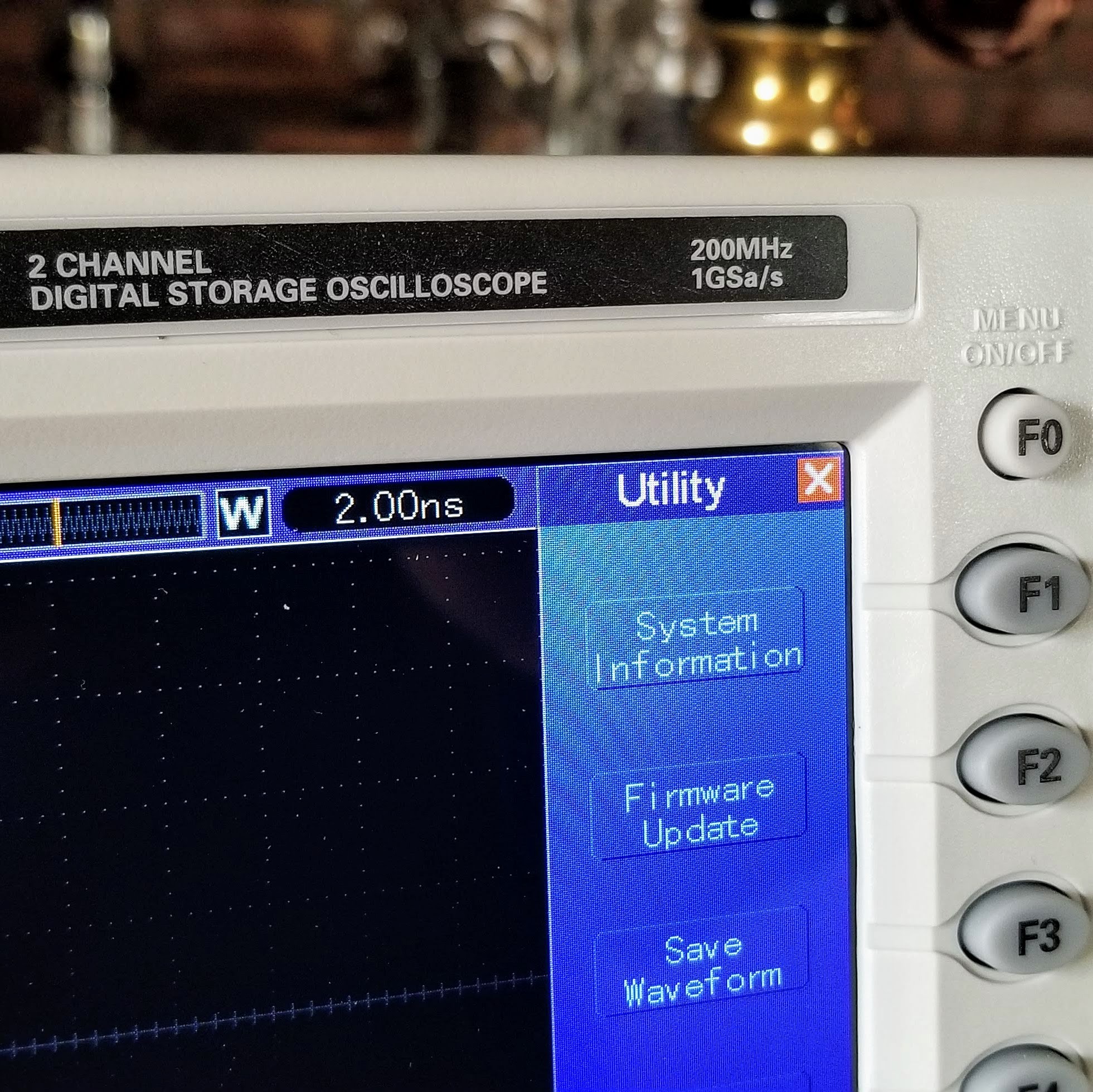
Needless to say, I’ve made some upgrades to my test equipment before I attempt the prototype!
![]()
Novasaur CP/M TTL Retrocomputer
Retrocomputer built from TTL logic running CP/M with no CPU or ALU