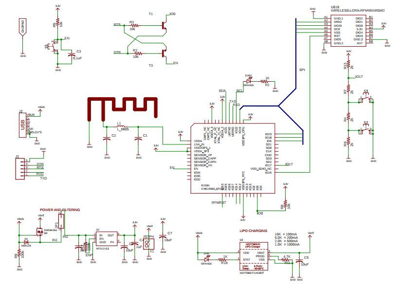
CORRECTION AND CHANGES TO SCHEMATIC.
It took a while for me to notice a "little" error in the previously posted schematic. I missed a pull up resistor for the buttons and misspelled some net names . Fortunately, I noticed it before starting the layout of the PCB. In my bid to correct the mistake, I thought it wise to review the components used with the device and made the following changes.
- I removed the OLED in a bid to reduce the power consumed and since all that it display could be inferred by other means (via LED and the PC/smartphone itself).
- I reduced the number of buttons to two.
- I added another LED for power and connection indication.

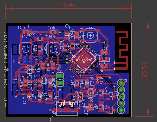
PCB LAYOUT.
I began laying out the components on the board with the aim of making the PCB as small as possible. There was a limit to its size as I used 0805 components for easy hand soldering ( I can't cope with smaller components ,YET ). I used the ESP32 Pico D4 chip for smaller size. The PCB measured 5 cm by 3.6 cm at the end.

The new schematic and layout has been uploaded in the project page. Off to JLCPCB...
 Taiwo
Taiwo
Discussions
Become a Hackaday.io Member
Create an account to leave a comment. Already have an account? Log In.