I really wanted to stay within the 2 sq in, or 13 sq cm constraint. Not just for cost, but for the challenge. I want the experience of laying out a dense circuit in Kicad.
Initially I assumed I could do a central hub with long arms sticking out that would be joined with solder once the components are installed. When measuring just the solid area of my designs, I could create a much larger mobius strip. It turns out that OshPark (and I suspect most vendors) measure your design by it's bounding box, or the smallest rectangle it will fit into.
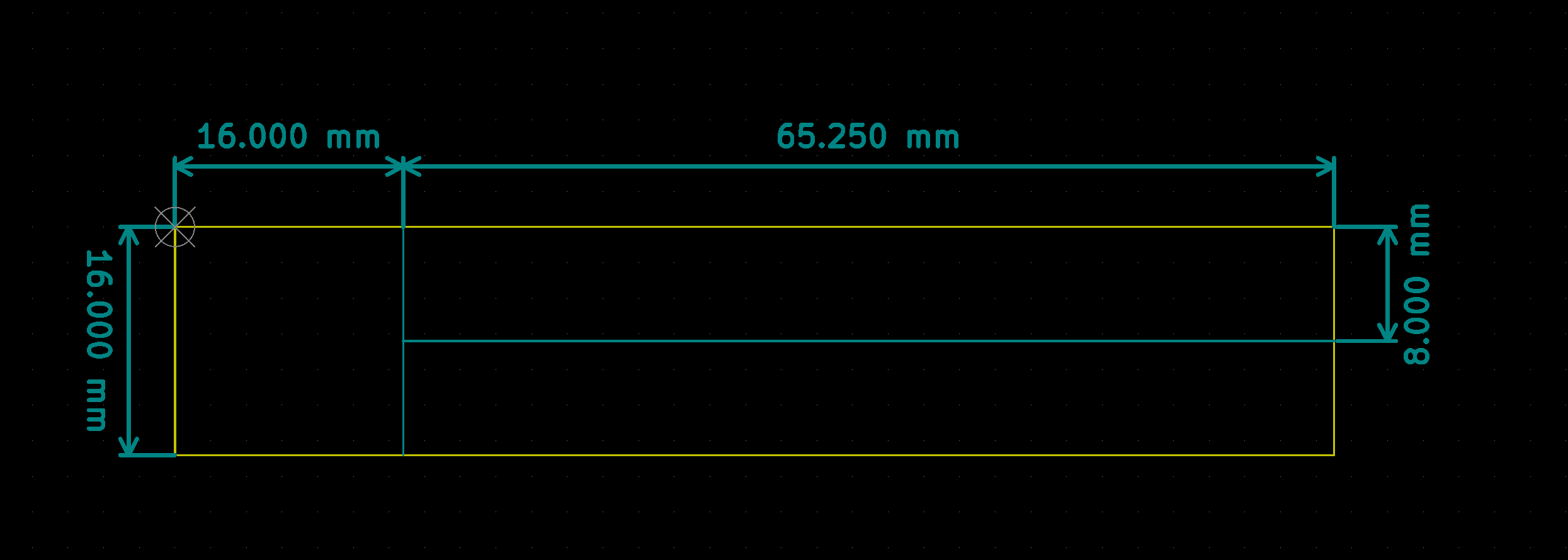
With this in mind I investigated layouts that could be cut apart, then re-assembled in a different configuration. I started looking at the minimum area needed for a central hub containing the microcontroller. Measuring an Atmega 328p QFP I had on hand, I found that this chip has a 12mm x 12mm footprint. This seemed rather large compared to 2 sq inches, so I decided to use the lead-less VQFN version of the chip. It measures only 5x5mm, which allowed me to fit my central hub including current limiting resistors and interconnects into 16mm x 16mm. At this point I also decided to use 0603 components instead of my go-to and easy-to-place 0805s.
Placing this at one end of a 16mm x 81.25mm rectangle leaves enough material for two additional strips, 8mm x 65.25mm. These strips will contain the LEDs on both sides, and will be soldered together, and to the hub, with the mobius twist.

 Chris Miller
Discussions
Become a Hackaday.io Member
Create an account to leave a comment. Already have an account? Log In.