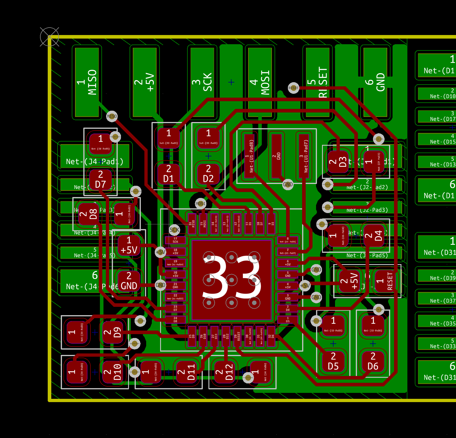
I had already decided to use the VQFN version of the Atmega328p on this design. That gives me plenty of IOs and a simple way to program it through 6 pins. I can also power the programmed device through the programming header's 5v and gnd pins.
Initially I thought the layout would be on both sides of the central hub. I was looking at multiple resistor packs, smaller components, both sides, etc... But it turns out that using 0603 passives, I was able to get the MCU, its supporting components, and 12 current limiting resistors on the top side of the 16x16mm main PCB. I used the smallest 6mil tracks and spacing that OshPark supports for flex PCBs. This allowed me to put all of the board interconnects and the programming header on the bottom for a clean look.

 Chris Miller
Discussions
Become a Hackaday.io Member
Create an account to leave a comment. Already have an account? Log In.