-
Feeling a bit stuck
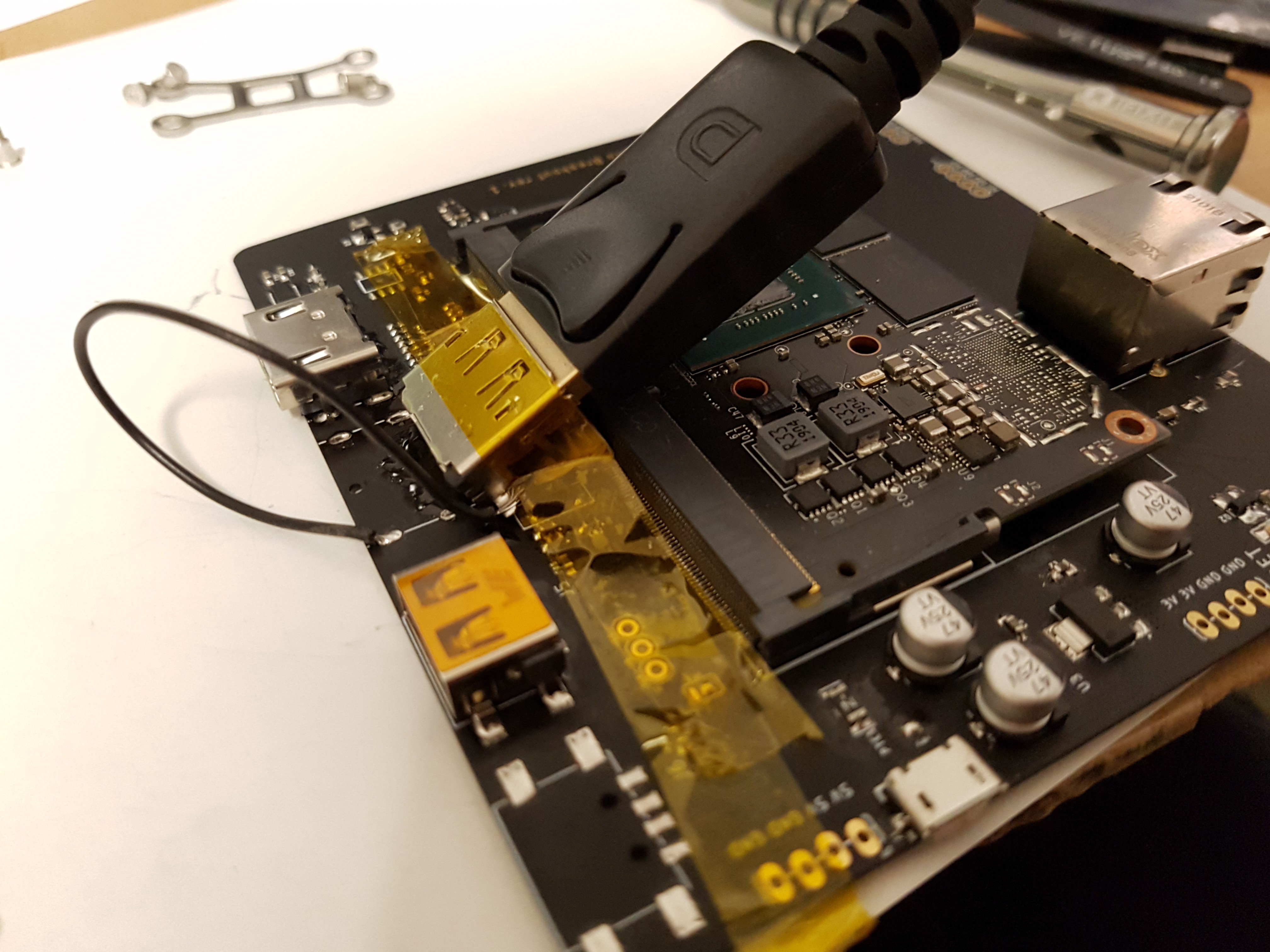
09/13/2019 at 21:42 • 0 commentsI haven't been very productive in the past few weeks. This was mostly due to me being a bit frozen with my eDP issues. I'm hesitant to move forward with the PCB design before this issue isn't fully understood.
Getting the display to work is quite important to me and right now I'm not able to debug why the seemingly same circuit, layed out with the same guidelines I used previously is giving me these issues. At the moment I'm reliant on Nvidia's support as I have no real starting point for debugging the issue atm. The pace picked up a bit on their side and after a few weeks of silence the hardware team on their side couldn't identify any real issues. The software team on the other hand found some odd behaviour in the link training. Link training is a feature of DisplayPort that consists of finding out the correct signaling strength and receiving display timing data from the display (similar to the EDID readout step in HDMI).
When it tries to establish a link the SoC does not try to up the voltage swing of all signal pairs but only for the first one. So most signal pairs stay at the lowest setting of 400mV, the first goes up to the maximum of 1200mV. This can mean two things, either there is a bug and because it does not raise the voltage swing for the other signal pairs it just fails over and over because it only touches the first pair. The other possibility is that everything is great with the other pairs at 400mV but something is very wrong with how the first pair is routed and the attempt of the driver to fix it fails, which atm seems unlikely but who knows.
What is so frustrating about this is that I know what to do next and have a pretty good plan to bring this project to where I want to see it but I'm held back by this odd ball issue and I can't do much about it.
I'm focusing on the mechanical side for now which can mostly be handled without advancing on the PCB design. I might still start with the newer PCB design as the production module for the Jetson Nano SoM is finally available which I had to wait for because the pin out changed there in relation to the pre-production devkit module. This new revision will feature the much needed reverse mount to the aluminium mounting plate which means I can finally get rid of this big silly heatsink.
In the next post I want to outline quickly what step I want to take in the next months to give you an overview of the development roadmap that I have planned so far.
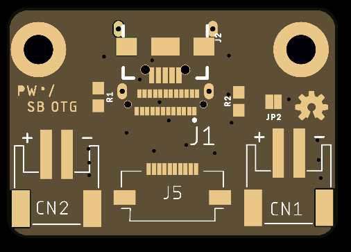
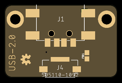
On the bright side, I came around testing the fixed USB PCBs and all is well now :)
Here it is happily talking to an Adafruit Metro M0.
-
Peripheral Bezels
08/13/2019 at 21:58 • 3 commentsThese are a solution to the fully customizable tablet version. If you read the project log about manufacturing I talked about having two different back cover plates essentially. One that is monolithic and neat, only usable for a fixed pre-selected set of peripherals.
The other would be the hacker, maker, researcher option that lets you fully customize position and amount (and kind) of peripherals, making it also easy to add you own custom hardware.The issue I had to tackle was how do you achieve this without having open sides or requiring 3D printing from the customer.
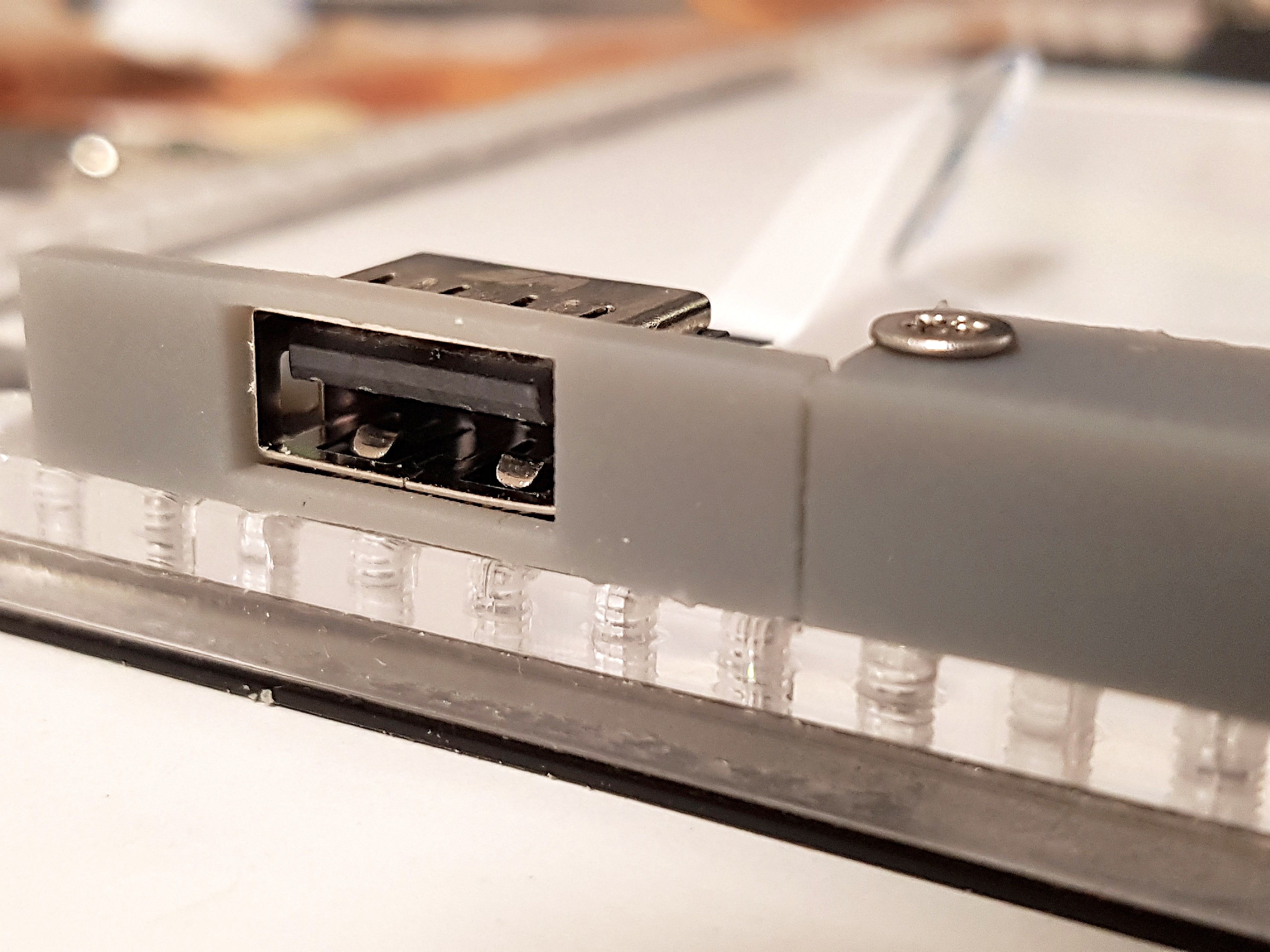
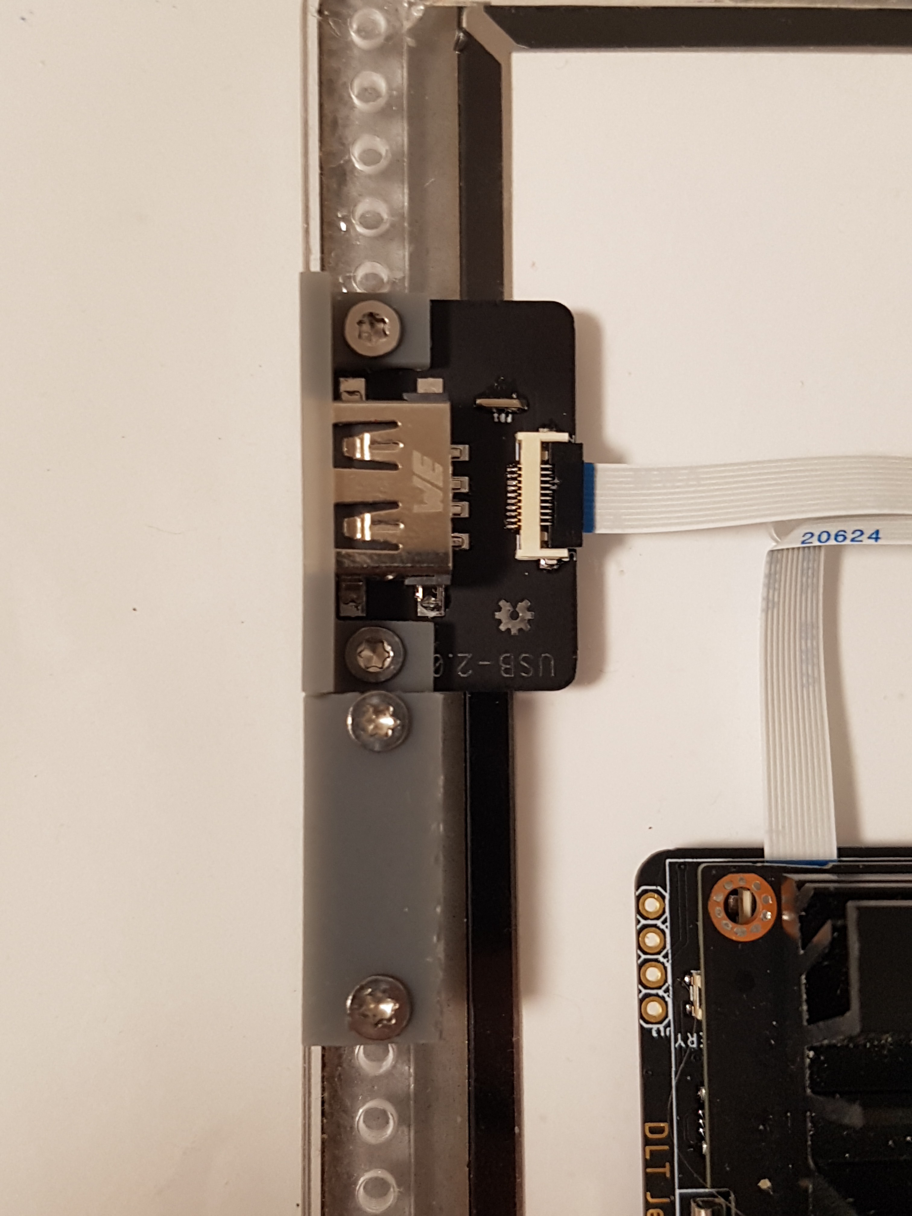
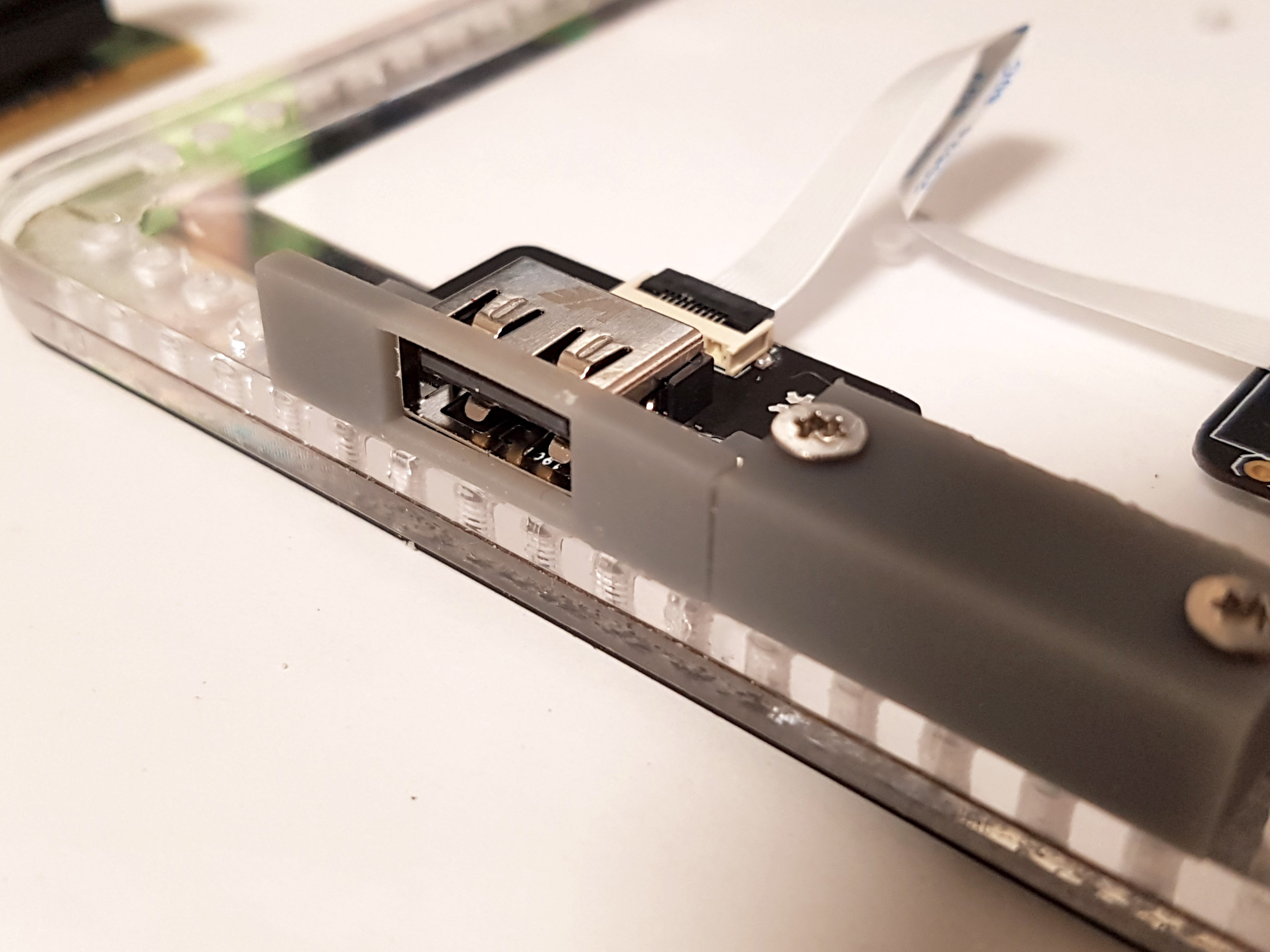
This is the solution I came up with (pictures below). Each peripheral will have to choose a bezel size. I haven't decided how many I want to include in the mechanical standard yet but it will probably be around 2 size options. They will only be allowed to differ in width, not height. Height is fixed for every element.
To close of the space between peripherals we have spacer blocks, they come in the same widths as the bezels, so if you have give amount of spacer blocks you can always make a closed side surface, even if you add your own peripheral, all it has to do is adhere to this mechanical standard.
The raster length is always a multiple of largest block width. The corners help define this, without them you will run into issues with different screen sizes, so the corners will always extend into each side of the tablet until they form this fixed raster length. That way you can adapt this to any screen size up to a certain minimum size given by the block width.
Finally some pictures of the prototype prints that I made for illustration. This will of course look much much nicer with injection moulded pieces and an aluminium mounting plate instead of clear acrylic :)
![]()
![]()
![]()
![]()
-
Mounting plate mock-up
08/07/2019 at 22:14 • 2 commentsI made a rendering of this before but I now laser cut a mock-up out of acrylic (the real deal will be aluminium).
It's purpose is mostly to test out how well the positioning of the peripheral works out and to experience any issues when working with a real display and PCBs. It's also the first illustration of the whole modular peripherals idea.
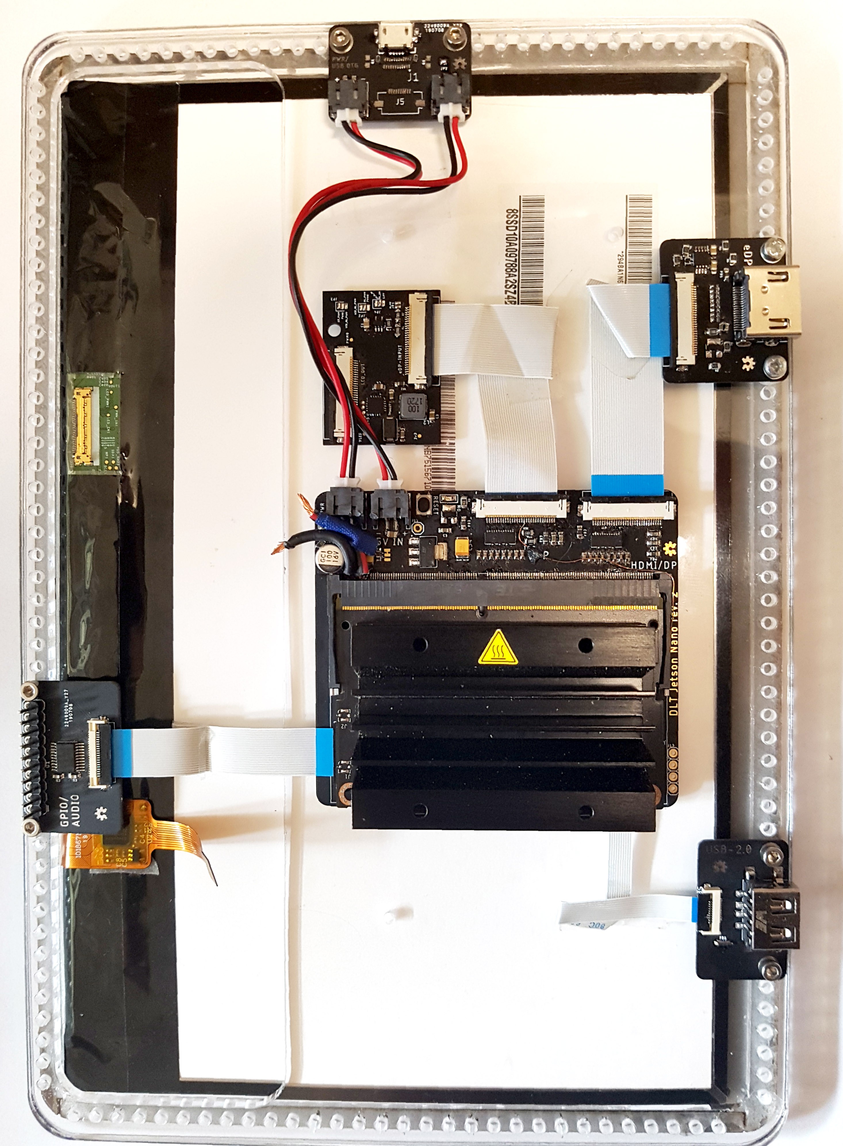
The result was quite promising. I also realized that I could slim down the thickness of the shim layer which raises the mounting plate high enough so it can sit just above or on the back of the LCD. I had concerns because there is always a part of the LCD that is thicker than the rest where the connector comes out (usually all covered up with black tape). I can just leave a cut-out there as the touch screen offers enough supporting area and lower the overall height of the shim. Here a picture of the whole mock-up assembly.
![]()
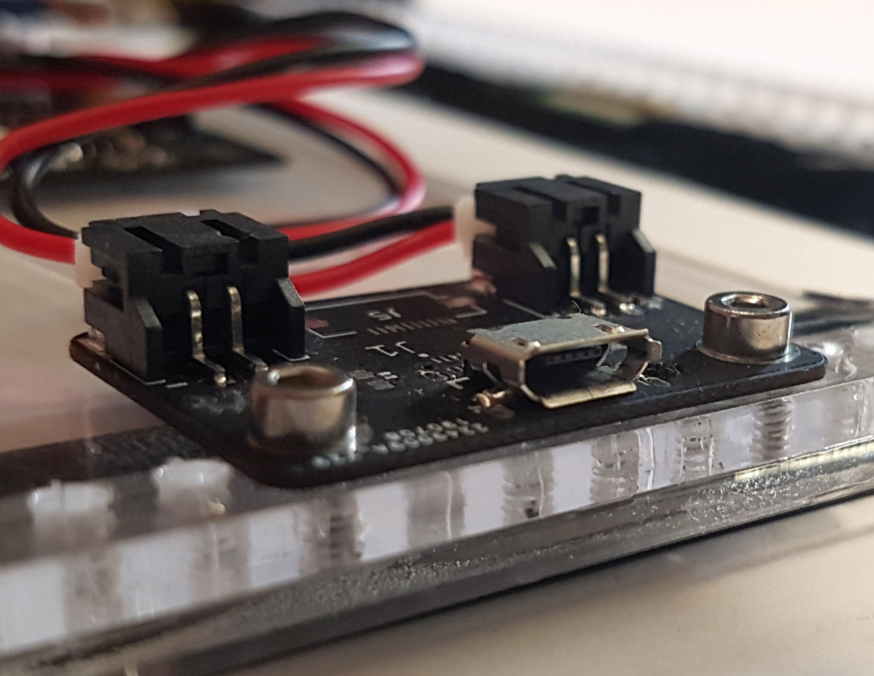
Placing the peripherals worked pretty well! The hole raster on the edge (and to a degree in the middle) is all threaded 2.5MM holes in a 5mm pitch. This gives nice even distances of 5mm increments for both positioning as well as hole placement on the peripheral PCBs.
Here a few close ups of some peripherals![]()
![]()
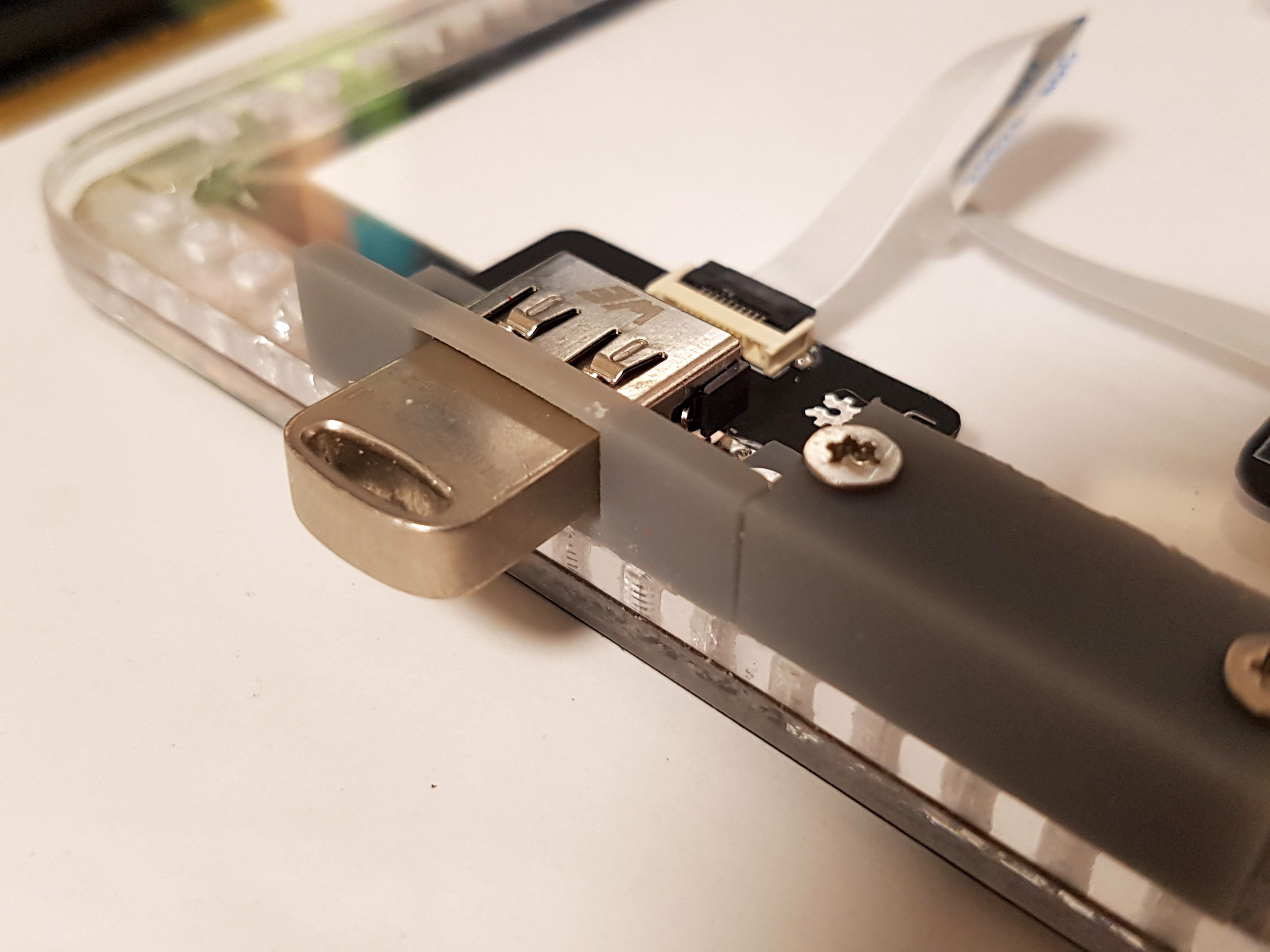
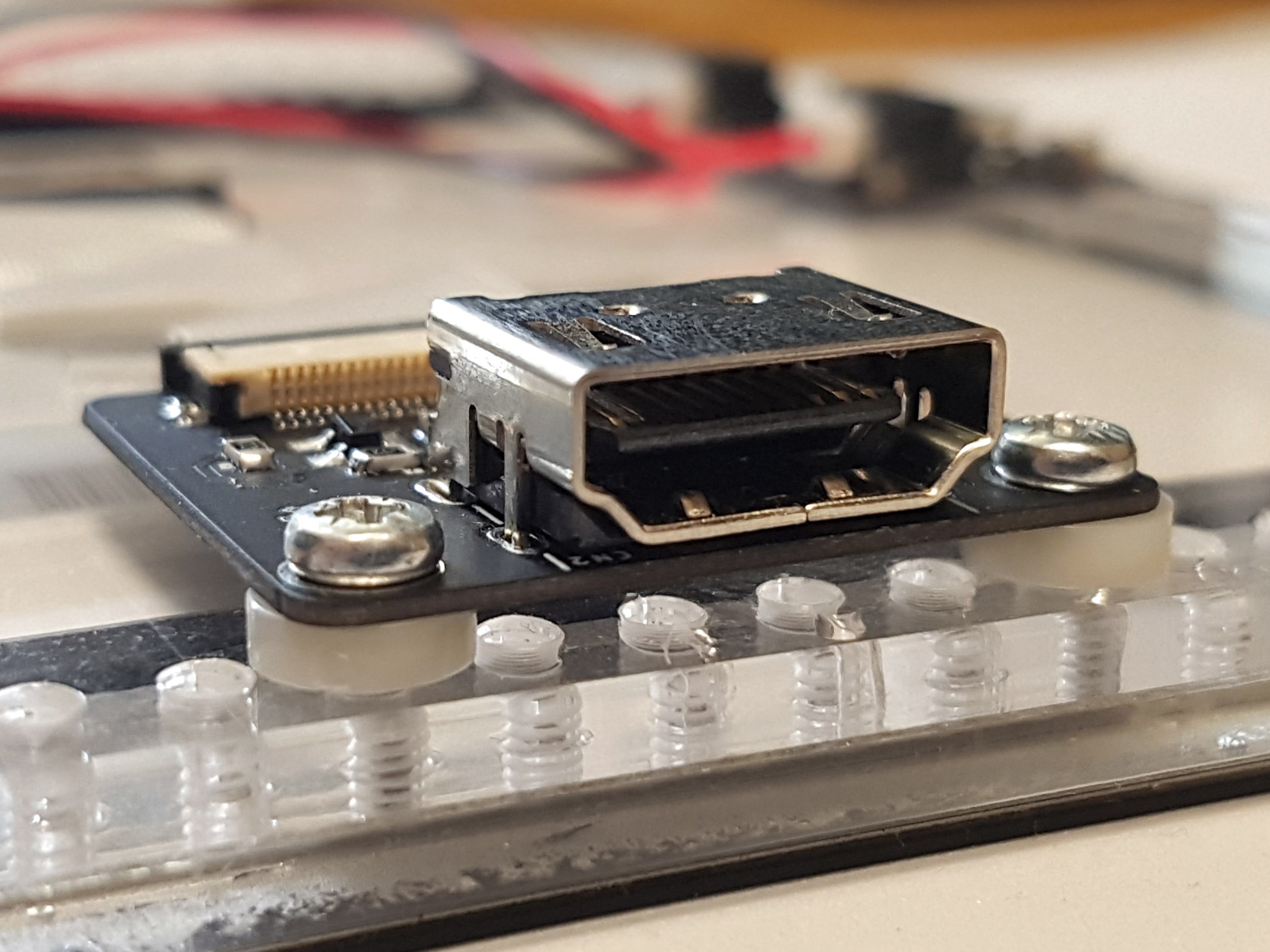
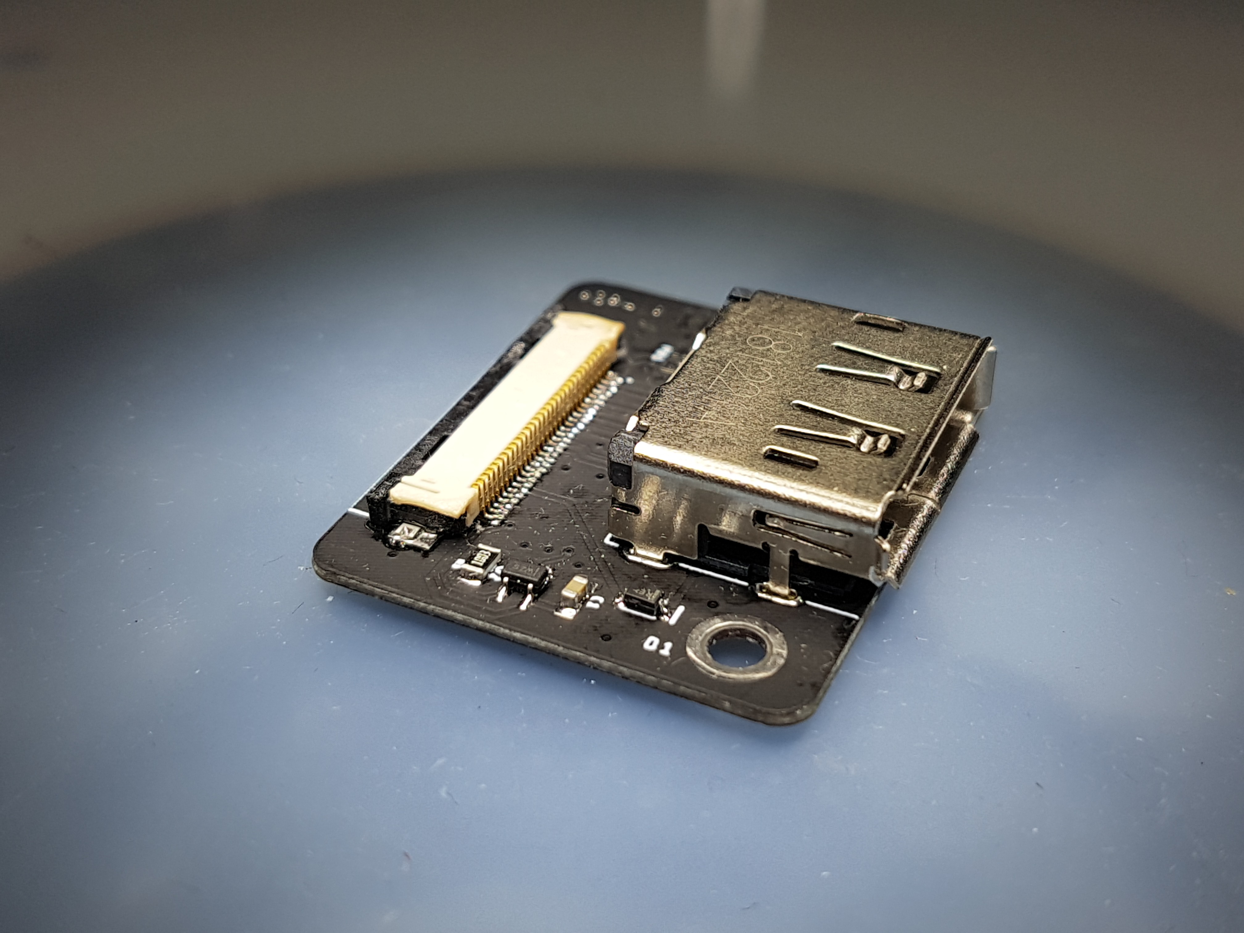
It is crucial that pure SMT components are used for this. With hybrid components like this HDMI connector below, you need spacers to raise them enough, those spacers are a bit too much but still, it will always add a 1-2mm to the overall thickness of the assembly.
![]()
This hopefully illustrate how the whole modular peripheral concept is supposed to work. This is of course an early stage but it shows where it is supposed to go.
As you can see there is always a slight offset from the edge for each PCB. This space is intended for the faceplate that each connector will receive and will make for closed side surface, even with a modularized back instead of a pretty but fixed injection moulded back.I will print mock-ups of these face plates in the coming week. So the next update is hopefully showing those off.
-
Problems with revision 2
08/07/2019 at 21:58 • 0 commentsUnfortunately the new revision had quite a few issues that I was not expecting. Revision 2 was largely a form-factor change, the circuitry was tested with the SBC style PCB in the first revision.
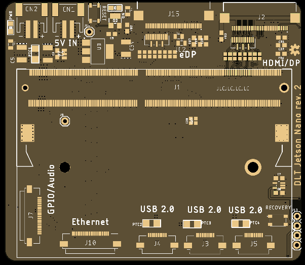
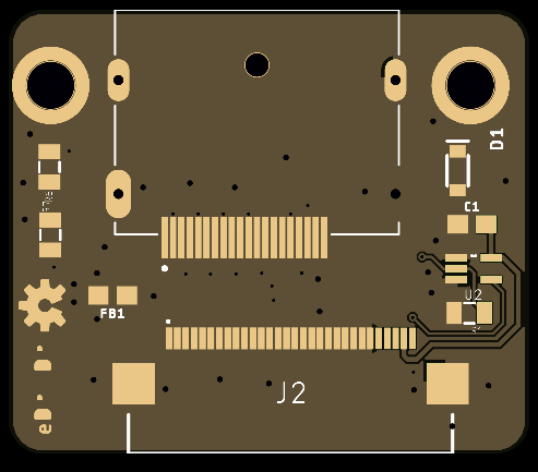
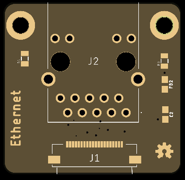
So what changed? Mostly that peripheral and most of the circuitry went on their own little PCBs and are connected via FFC to the mainboard which now has a much more reduced circuitry, that brings costs down for the mainboard and you only pay for the peripherals that you actually need, this also enabled a free positioning of the peripherals but more on that in the next update.
Back to the mainboard. When I powered it on with Ethernet attached I got no device showing up in the network unfortunately. When I attached the serial console I got at least a boot log so things were actually running but it seemed kind of flaky, I often didn't get a login prompt at the end of the boot process. At the time I was thinking I was having power issues but in retrospect I think this was just a bug in an older version of JetPack (the OS for the Jetson, a modified Ubuntu).
I turned to the schematics and realised that the pinout on the Ethernet FFC connector was shifted by one pin to the right...
The same happened to the USB which I tried next with an Ethernet dongle but had not luck either for the same reason, pins were offset.I was really puzzled about how that happened until I realised that the tabs of the connector which carry no signal were on the same side as the actual data pins on the schematic. When I mirrored the pinout I just mirrored it and applied it to the connector again in reverse order. The issue was that I included the tabs in that process and assigned them a signal instead of the GND connection...
![]()
Oh well, fortunately not the most important peripherals for now and I learned a (circuit) life lesson.The eDP and HDMI connector pinout were fortunately all good, I took a bit more time on those and didn't rush them out in day like the other peripherals.
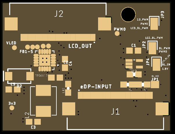
Unfortunately they didn't work either. At that point it got quite frustrating, I went from a 100% working revision to a 10% working revision.I quadruple checked everything, first thing I found was that I missed the eDP hot plug signal, it got renamed in the whole moving process. This was quickly fixed with a bodge wire. At that point the Jetson tried to establish a connection with the display and did seem to communicate but always failed during the link training process which establishes certain ground rules with the display for how the connection will be handled. The equivalent to this in HDMI is the EDID readout with the addition here that there is also some negotiation about the amount of signal lanes to use and other timing related things.
I did not get any further with this unfortunately. I tried wrapping my FFC cable in copper foil to shield it. I used shorter DisplayPort cables. Nothing worked. I got contacted by a person from Nvidia that also already helped me before with design resources, so hopefully I will get some more insight there of what might be wrong. Again, the circuit did not change, its all the same.
HDMI was a similar situation, EDID read fails but fortunately the Jetson goes into a default resolution for the HDMI for some reason if it can't read the EDID and this gave me a picture! So that at least hints that its not an impedance issue introduced with the FFC cables.
Why does the EDID read fail? I do not know, I checked the circuitry surrounding the I2C signal level translation but could not find any issues introduced with the move.
It is interesting though that both fail at a similar stage, the EDID readout / link training.
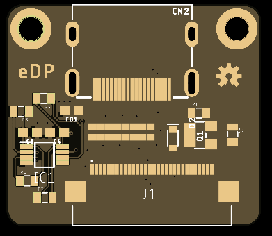
I tried the actual eDP PCB which connects to the eDP panel instead of a DisplayPort display. Unfortunately no difference, here I get even a stranger behaviour, the Jetson does not boot at all. When I unplug it and reset it is booting fine again. Hot-pluging it 'works' it atleast doesn't crash the system and yields similar edid / link training error messages as with the eDP to DP PCB.
While I'm waiting for feedback from Nvidia I started mocking up the mechanical design ideas. Specifically the central mounting plate. More on that in the next update.
-
Revision 2
08/07/2019 at 21:25 • 0 commentsI've been busy the past few weeks.
I held back a bit with this update as I wanted to get certain things finished and some things debugged first (which wasn't successful yet).You could follow along with my daily struggles on twitter if you are interested in more regular updates. I use this blog more for the condensed version every couple weeks.
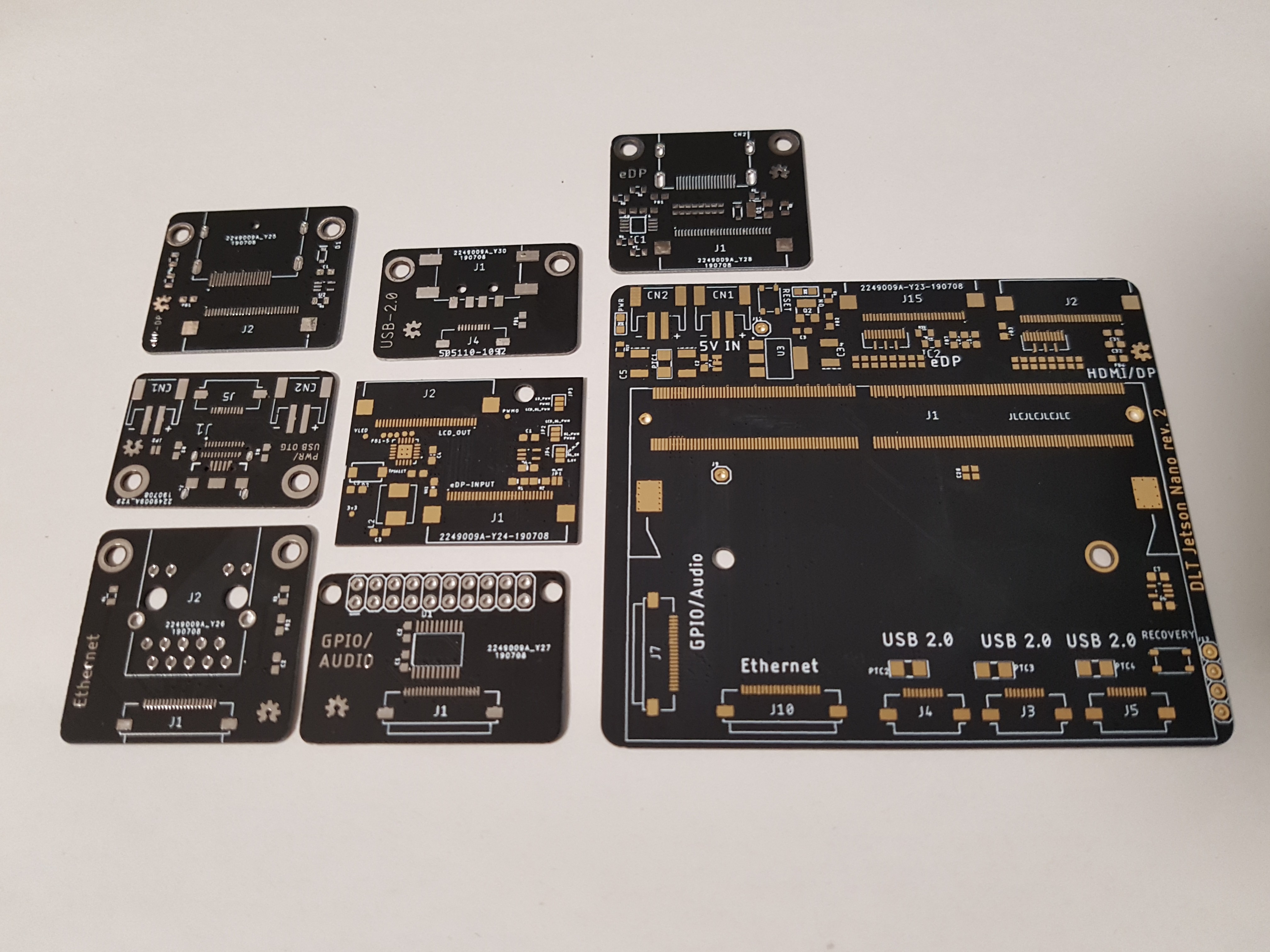
The boards arrived a while ago from JLC, again in matte black which now comes at no extra cost which is quite nice! I know PCB business cards are a bit dated by now but you could get them now in glorious matte black for 2$ which is just insane...They were also supportive and sponsored a large part of the order which I think was the largest PCB order, in terms of different designs, that I've ever done...
Here a shot of all of them together.
![]()
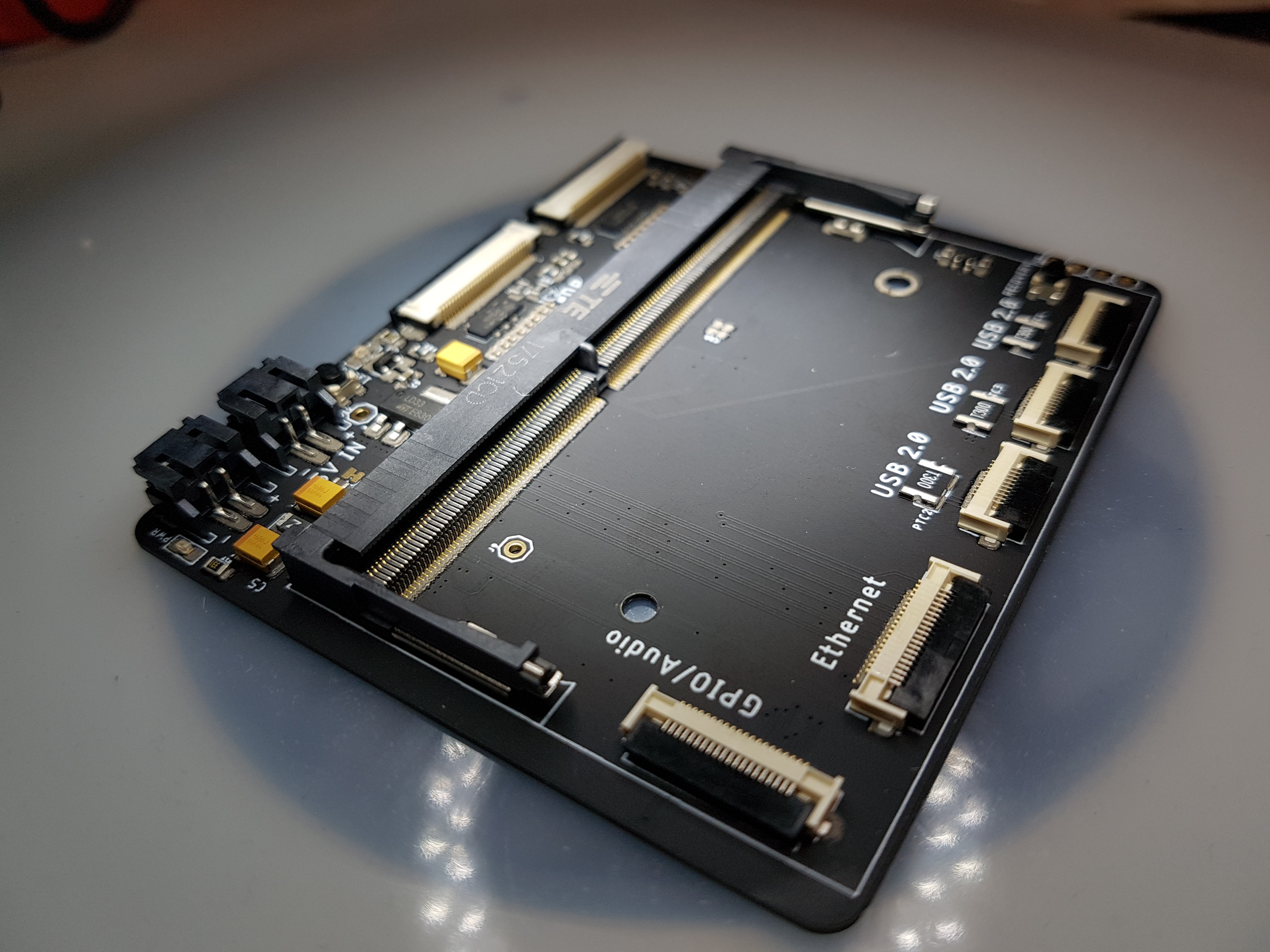
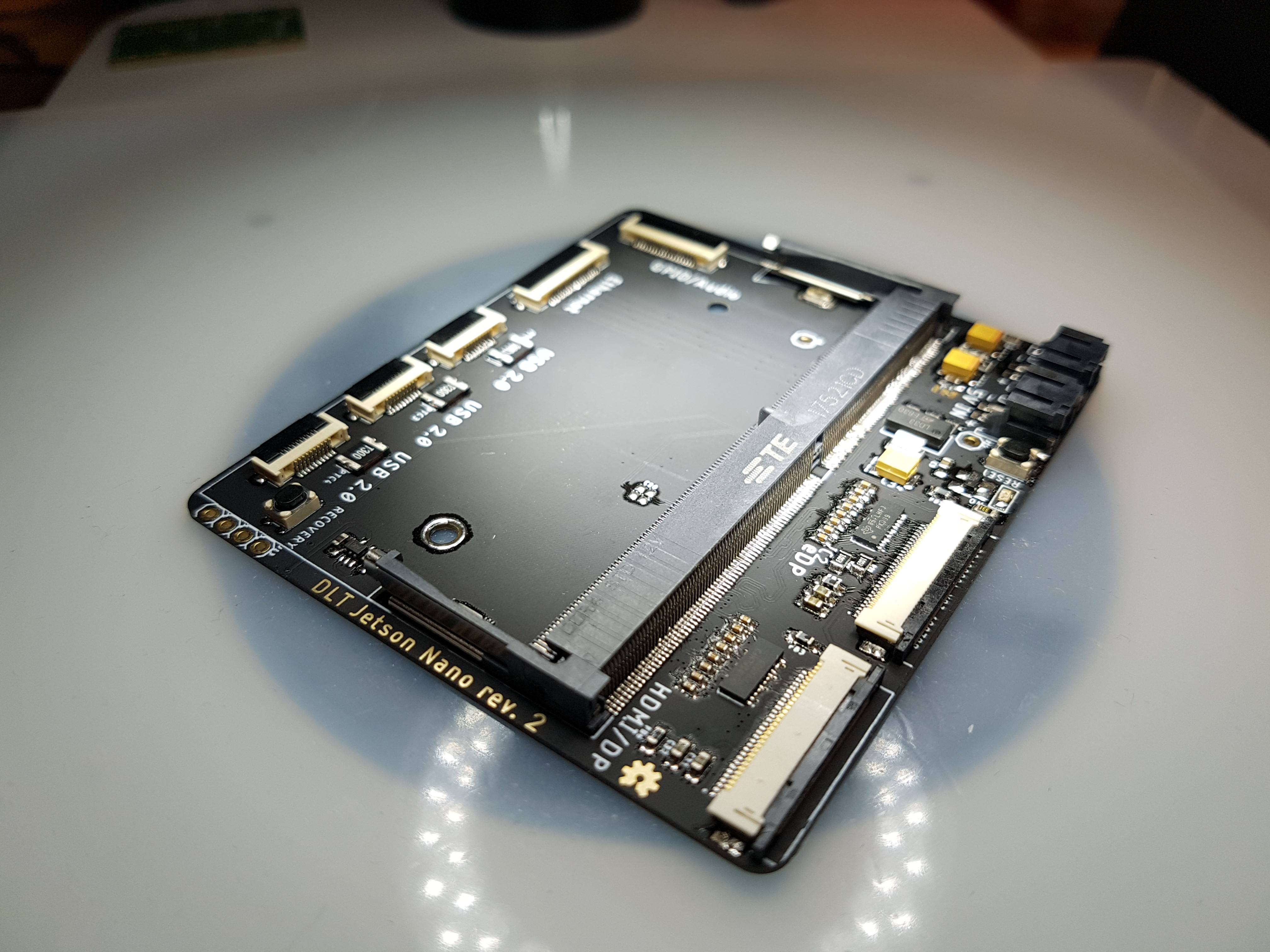
I got to populating the mainboard first, here a few shots of before and after reflow.
![]()
![]()
Got quite a few shorts which was annoying but nothing that the soldering iron couldn't fix.
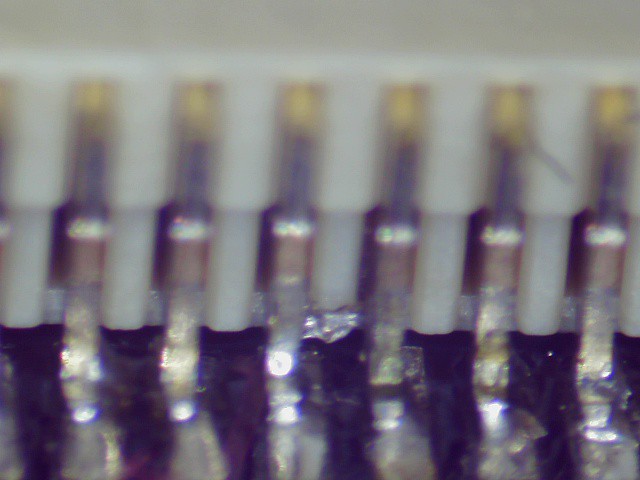
Except for this little fellow which gave me quite a headache before I discovered it. It was shorting 1.8V with 3.3V...
![]()
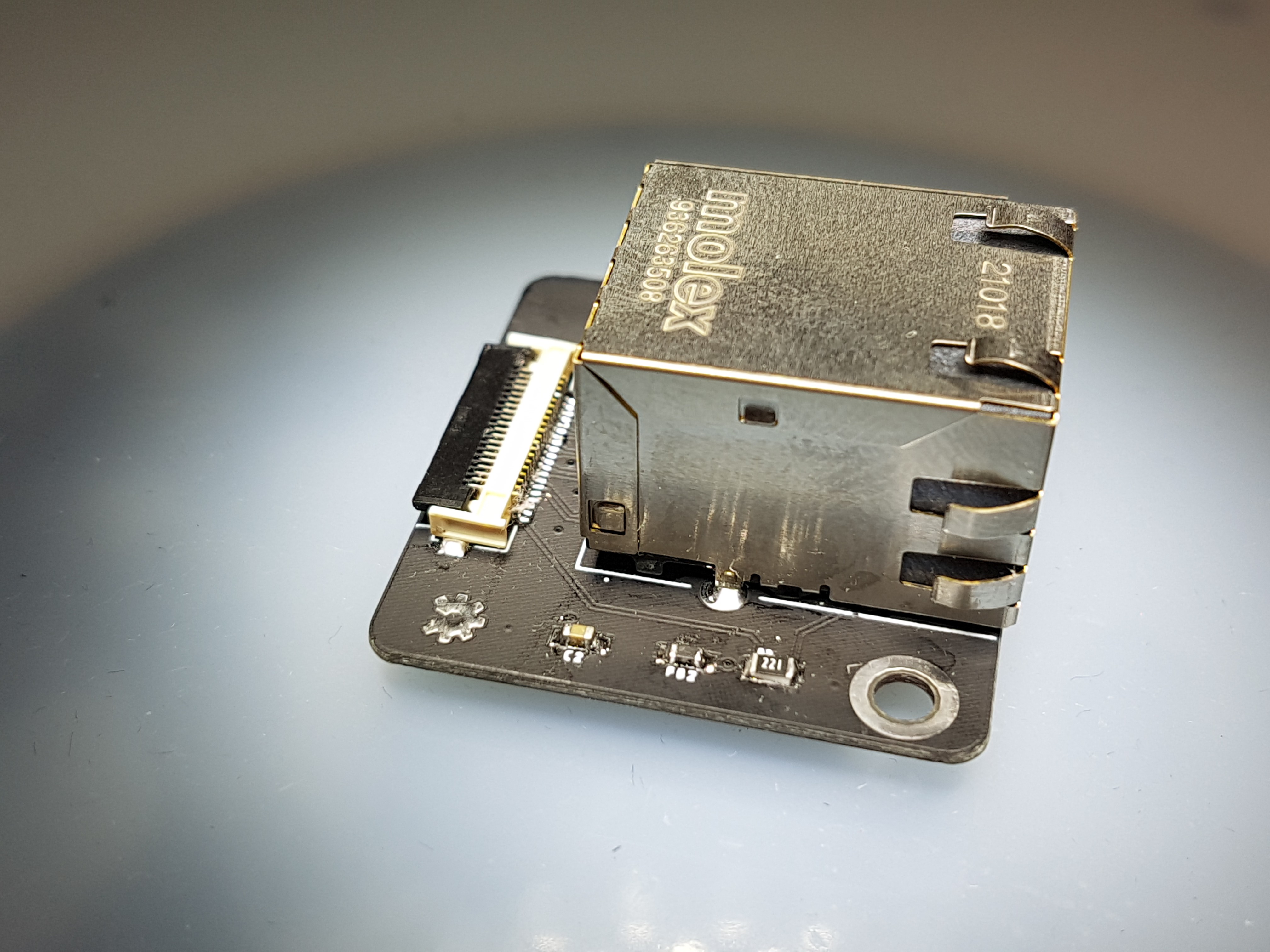
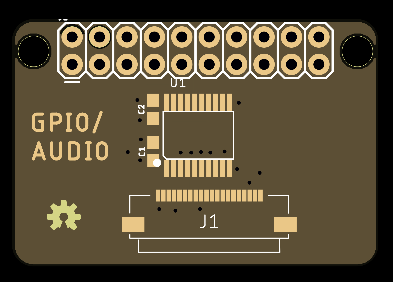
And another shot of an HDMI peripheral board as well as Ethernet (not really considering Ethernet for a final version but its great for debugging)
![]()
![]()
So how did it go you may ask? Not very well unfortunately. More on that in the next post (which will come out in just a few minutes)
-
Manufacturing and the target audience
07/08/2019 at 23:17 • 4 commentsA topic I haven't talked about in too much detail yet.
Its something I'm constantly thinking about whenever I change something in the design. The tricky part is that I want to reach two main target audiences which require somewhat conflicting mechanical design.
The first one being the general open source crowd, no matter if they are interested in hardware or not, there is quite a lot of interest from people who are interested in Linux and open development. They mostly want to see a tablet that comes close to a polished commercial tablet, from the feedback I've got it seems they are fine with something thicker but it didn't seem there was a ton of interest in fiddling with hardware or getting something that works but looks ugly. Small to mid sized industrial companies are also pretty interested in something like this, they would require a more rugged case and are also fine with thickness but also require a finished and polished product that is well integrated.
Catering to this crowd is actually not hard, you require a few injection moulded pieces of plastic (I try to keep it as simple as possible, so far I see about 2-3 large pieces of plastic) and make a design that is constrained and tries to squeeze the hardware into any space there is to yield a tablet that looks nice and tidy, just as a tablet would look like that you bought from the usual Manufacturers. Sure there will be a few iterations until it comes out perfect but injection moulding is a well understand process and can be done in any quantity now a days. There is polyurethane casting for prototyping and small runs of 10-100pcs.
Next step would be injection moulding with an aluminium tool, they are a lot cheaper to manufacture than the high-end steel ones and yield y few hundred to maybe 1k pieces and if you are going really big you can scale up to steel tools and produce several 10k-100k per tool ( I pulled those numbers out of my nose but this is the range I remember).
The issue is that I can't design the mechanical parts so that they are only feasibly manufacturable with injection moulding.
This is because I have a second target audience that I personally find most exiting and is what drives me personally. It's the hardware hacker crowd, the educational crowd, the mid-size company that wants 10 super specialized tablets that integrates their own weird oddball hardware.
Those people want to modify the hardware, they want to experiment, they want to make their own spin-off.For this audience I need to think about hack-ability. It doesn't mean they don't want a somewhat good looking tablet, but extendability is key here.
This is one reason why I design the electronics in a very modular way, no peripheral is fixed, everything is changeable. Don't need HDMI output? Then don't get the HDMI PCB. Need it 2 years later? Just buy it for a small amount and add it to your tablet, no need to buy a whole new thing. This not only allows upgrading to some degree, it also allows for great repairability which is something pretty much everyone likes.
Now there is a catch here, how do I add an HDMI port to a case that doesn't have an opening for it?
This why I decided to design the case in the following way. There will be a display assembly that consists of LCD, Touchscreen (the two will not be bonded for repairability) and a plastic 'spacer' that creates a frame around the LCD. This assembly is then acting as a flat surface where the aluminium plate will be attached to.This plate will have a sort of pegboard pattern of 2.5mm threaded holes where the electronics can be attached to, this allows for free placement of all peripherals and the motherboard. This plate can be easily manufactured in lots of different processes, its thin enough to be done in a sheet metal process, using water-jets or lasers, or more expensively, on a milling machine.
The tapping will be a bit more expensive than just having threads in a limited amount of places for a fixed set of peripherals but this can be done with CNC (not actual milling) and is a standard part of a sheet metal workflow.
So far so good, none of these parts need to be exchanged if you were to change a peripheral or anything else in the electronics design.
Only the last part gets tricky, its the back. This is a plastic piece that will serve as nothing but the cover for the electronics, nothing will attach to it, it just covers it up. It's also the driving factor of how the the Tablet will look.
The way I have the design in mind so far is that this back can be produced either in a high-end manufacturing way (e.g. moulding) or in a home shop through 3D printing or milling, heck even laser cutting can work, you just need to laser spacers to put between the peripheral connector and have one large plate cover everything up.The possibility for easy prototype manufacturing will be important for testing out your own variants of the tablet, this is important for business users and of course hackers.
There is a not so small market that is in need of very specialized portable electronics where a tablet is 90% of what you need but the remaining 10% is their own specialized hardware that they just need to integrate into the tablet, DLT will serve as a perfect basis for these kind of projects.Now back to our average Linux lover who wants to add an HDMI port because his needs changed.
I want to offer him several ways of doing that, one I just described right now, visit your hackerspace and make something yourself. That's something very few will do but they have the option.
The next option will be getting a new back, maybe you opted for the integrated back cover before, unfortunately you will have to ditch this, right now I don't see any feasible way around this but you can keep the most expensive and resource hungry parts of the tablet.You will then have to get the second variant that I plan to offer, it will be similar to the first but the sides of this variant will be open except for the corners, the corners are where the large screws go in, to hold everything together (look at the early mechanical design concept for a visualization).
Now you can get a set of pre-made 'jackets' for each peripheral so they are encased nicely and a set of spacers that fill the holes between the peripheral connectors, this allows for a pretty free placement so everything is located where you want it to.These spacers and jackets will be screwed down onto the aluminium plate just like the peripheral PCB's. Thanks to counter sunk screws they will end flush and you can put the finishing back plate onto everything just like you did before.
I'm not sure if I will go with these two variants, maybe I will only make the customizable one, this really depends on how much my customers are willing to do some end assembly but from the current feedback I feel there is a large crowd that will be happy with a minimal set of peripherals and a finished product that requires no assembly and for those the cheapest and easiest option will be a 'unibody' plastic back.
Of course there is also the possibility of made to order tablets where the customizable variant is build for you but this will jack up prizes and is not something I see as viable in the near future.I try to add some picture to this blog post later on to illustrate the concepts better, for now the wall of text has to suffice :)
I focused solely on the mechanical manufacturing part here, getting PCBs assembled is something so standard I don't think I have to go into details here. There is nothing particular unique in terms of parts for DLT. -
LCD and Touchscreen combo
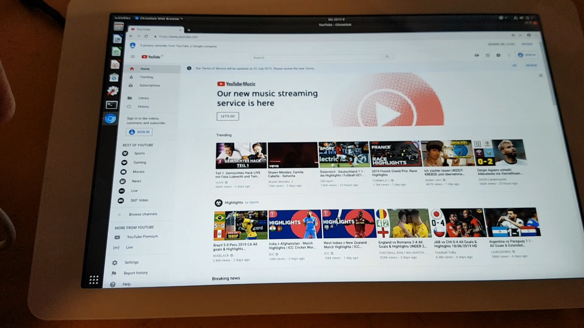
07/07/2019 at 20:46 • 0 commentsI got a nice 8.9" eDP LCD and a fitting touchscreen with a glass cover in typical tablet style, they only got white in stock, I would prefer black for future tests but it works well for first tests. Touchscreen was working perfectly in Ubuntu out of the box.
![]()
![]()
-
Revision 2 ordered
07/07/2019 at 20:34 • 0 commentsIt's been quite a while since the last update. Some private events kept me busy for a few weeks and I had somewhat of a slump, the second prototype was all about defining sensible pinouts for all the FFC's, finding out what connectors to use, what pin counts, what problems could arise in different applications than mine with the pinout I'm choosing and lots of other little decisions.
It's important work but can feel a bit like a drag because you essentially just redo what you already did in a different way.
I've worked through the slump and churned out a new motherboard and over the weekend I made 7 little peripheral breakouts.
This will be the first proper proof of concept. The part I'm most anxious about is the eDP to LCD part, I've never talked to eDP LCD directly before, so lots of stuff I could have missed.
Now that I'm waiting probably about 2 weeks for all those boards to arrive I will focus on milling a prototype aluminium frame to attach these PCBs to. I also got a nice LCD and touchscreen from a vendor, more about that in the next post.
![]()
![]()
![]()
![]()
![]()
![]()
![]()
![]()
-
Found all the bugs, working on next design
06/12/2019 at 21:17 • 1 commentSo turns out I simply forgot to connect the AUX_GND pin for the DisplayPort connector, a quick bodge wire and DisplayPort was working as well :)
Ethernet is only 100Mbits because I mixed up the connector pinout. Molex had two versions for the part that I used and for some reason the bi-color MagJack has a different pinout for the diff. pairs rendering 2 pairs useless which makes me end up with just a 100Mbit connection.
I have ordered the correct part for the pinout and will see if it works ok after reworking it.
I'm currently in the process of designing the next prototype which will be the actual first prototype meant for the tablet instead of a SBC like before.
It will be as compact as possible and breakout everything over FFC like I planed. This also means I have to spec the electrical standards for each peripheral. This will probably not be final but its important to keep future solutions in mind here already. After all its supposed to be a universal standard for portables, not just for my initial tablet here.I expect this to take another 2-3 weeks as I wont have too much time due to private life stuff.
But I want to see it assembled in mid July and maybe do a second revision before the judging deadline in late August.
-
It's alive!
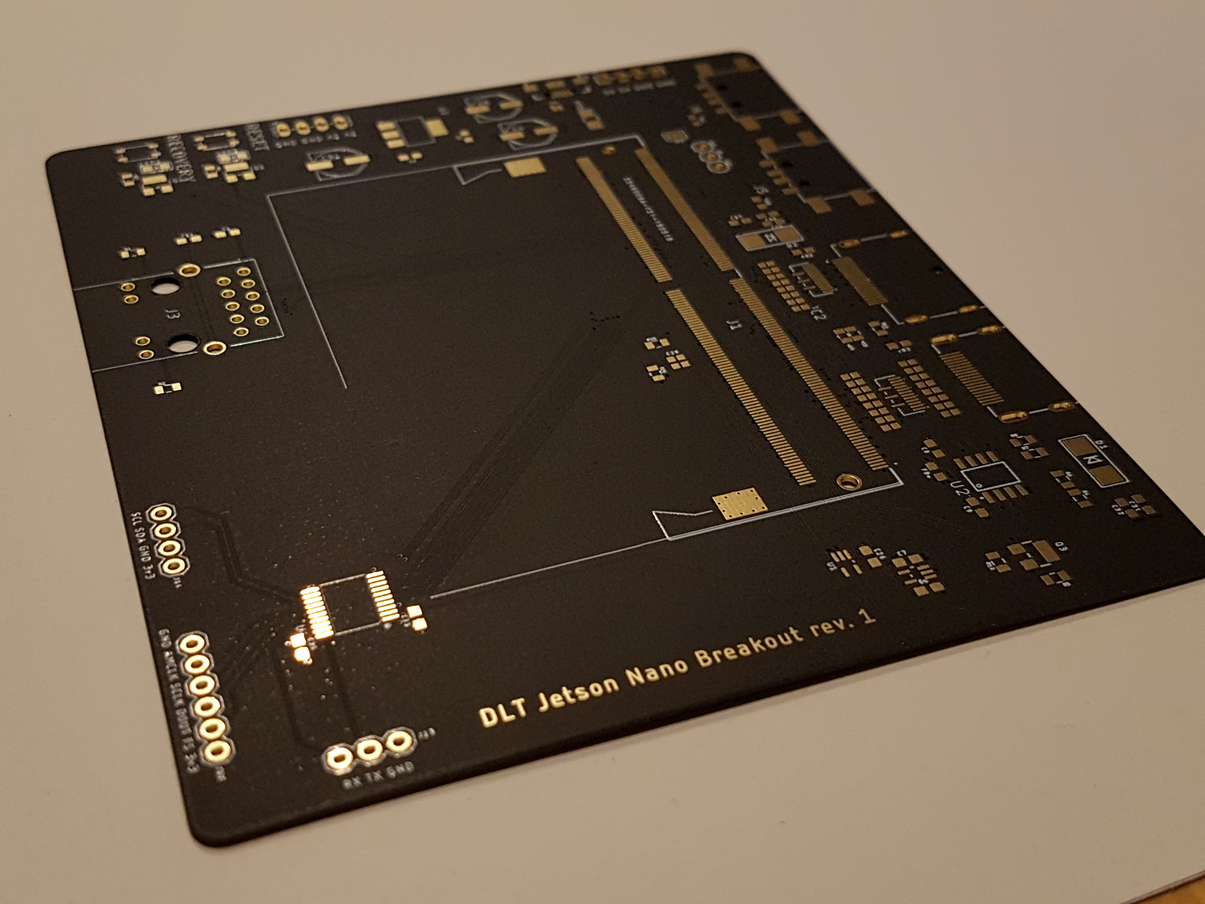
05/28/2019 at 22:25 • 2 commentsSo the PCB came yesterday and it looks super pretty! It's a 4 layer board with impedance control.
Also thanks to JLCPCB for sponsoring the board.![]()
The best part is, after soldering it together, it was actually working! Well everything except for DisplayPort.![]() A friend suggested that I used the pin layout for a DP Sink instead of a DP Source. Who knew that existed! So you have the layout reversed depending on whether you transmit or receive the signal.
A friend suggested that I used the pin layout for a DP Sink instead of a DP Source. Who knew that existed! So you have the layout reversed depending on whether you transmit or receive the signal.
I tried reversing the connector but that unfortunately did not change anything. Will have to further investigate why.![]()
DLT one - A Damn Linux Tablet!
Modular Open Source Hardware Tablet that is easy to hack and can run a standard Desktop Linux Distribution (or Android)
 timonsku



 A friend suggested that I used the pin layout for a DP Sink instead of a DP Source. Who knew that existed! So you have the layout reversed depending on whether you transmit or receive the signal.