-
Mechanical Design
05/25/2019 at 22:03 • 1 commentI haven't talked too much about the mechanical side yet, which I want to change now. I did some sketches in Fusion to illustrate what I want to do here.
I want to make the mechanical design akin to how a PC case works. So it is a generic mounting point and shell for the hardware, you are able to change hardware without also buying a completely new case.
This is a bit tricky when you have so little room like in a tablet but it is doable to a degree. I want you to at least be able to swap out peripheral connections or add/remove them. Maybe you want a 6.3mm Audio Jack because you are an audiophile or you want a GPIO header on the side for hacking on the go.
I want to keep the amount of parts needed to a minimum. This keeps costs down especially when manufacturing the project on a larger scale. If only have to buy tooling to 1-2 plastic pieces that saves a ton of money for smaller production runs.
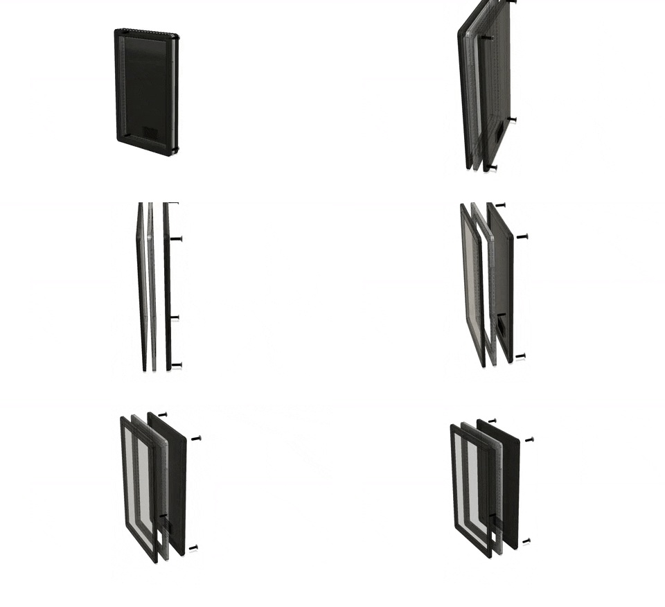
The frame is made out of 3 major pieces at the moment and is hold together by 4 screws (that might change as it is likely that is not stiff enough on the long side of the tablet).
Here an exploded view of the current design. Bare in mind that this is still largely conceptual and it misses some details like studs that will be needed for stability of the back f.e.![]()
The back is hollow and offers room in addition to space the aluminium mounting plate already creates.
This gives me 7mm space for hardware at the moment. I might have to increase this to 9-10mm by increasing the tablet thickness but I would like to avoid it. At the moment the tablet would have a thickness of 14mm which is about 2012 era tablet thickness. Which is still absoultely ok for me. This makes the product more hacker friendly (and repairable!). If you are looking for a 7mm iPad you will probably just get an iPad...The idea with the mounting plate is that it defines a mounting standard similar to that of expansion slots in a PC case.
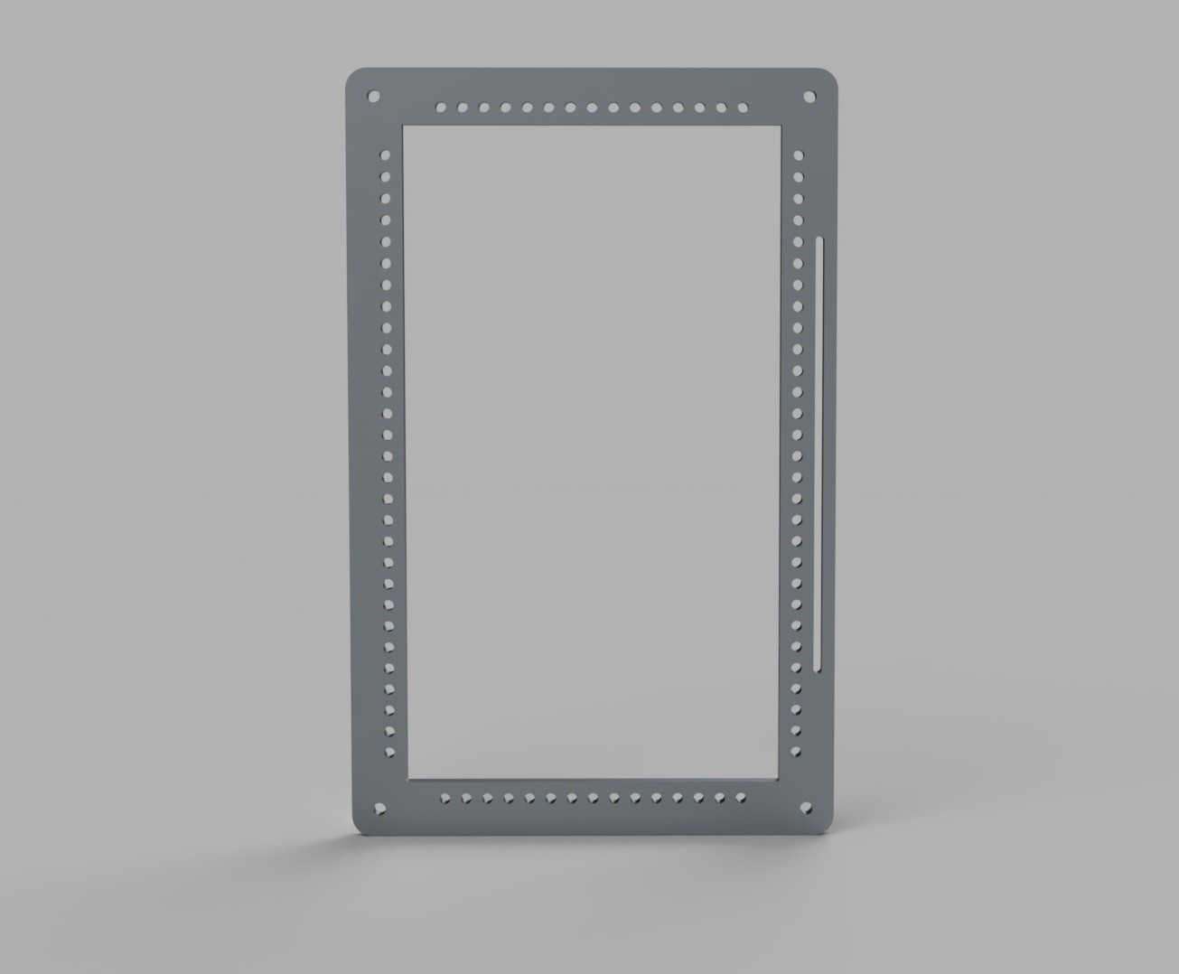
It has M2.5 threaded holes which are spaced 5mm apart giving you a nice even grid of 5mm steps.
There you can attach small PCBs for the peripherals that you wish to use (as well as the mainboard through another small mounting plate that takes heat away from the SoC to the large mounting plate).The mainboard will offer several FFC connectors that break out all relevant peripherals. So each peripheral will connect to the outgoing connector through a flat flex cable.
This makes the mainboard itself very compact and you have the total freedom of where you want to have which functionality!
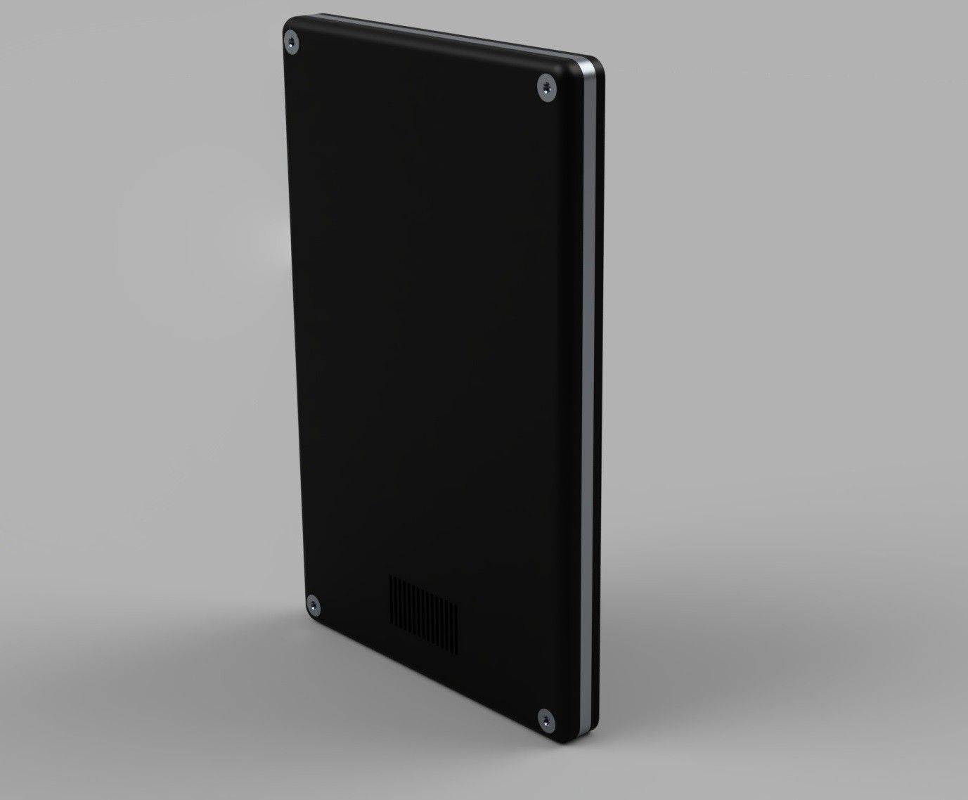
The only thing you would have to re-do is the plastic backplate. There are two options here. Have this be constructed out of one large back part and several smaller spacer parts that you could put between peripheral PCBs to close up the sides.
Or you have a single piece and you will have to print or mill yourself a new one.
From a product perspective I might offer both options. The latter looks much nicer, the former is more hacker friendly but actually very cheap to produce. It would actually make it possible to laser cut the whole assembly.
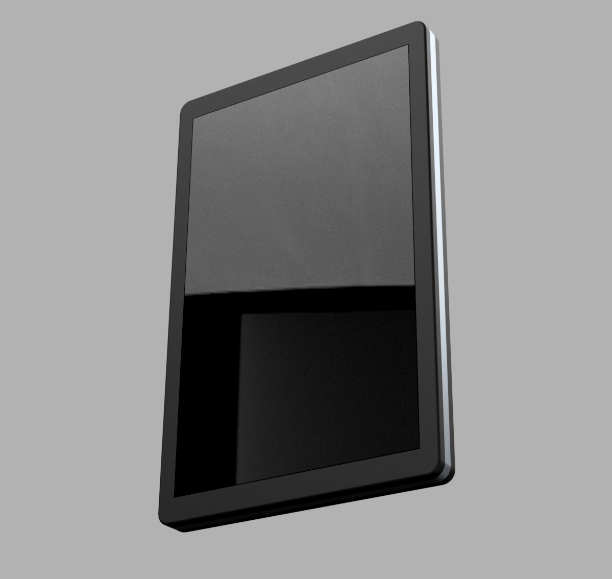
Here are some renderings. I'm still missing some dummy PCBs, I will add those in later to make it clear how the whole modular peripheral thing is supposed to work.![]()
![]()
![]()
-
Switching to Jetson Nano
05/18/2019 at 16:27 • 1 commentAfter being rather frustrated with the state of documentation of the i.MX8M SoM and sparse design guide I'm now switching my efforts over the Jetson Nano from Nvidia.
Among my main reasons why I will pause my efforts with the i.MX8M is the availability of a polished end-user Linux in the form of L4T (slightly modified Ubuntu), with the i.MX8M you get a lot of options but none are really meant as a finished piece of software for end use but as a base for your own build. This is great for someone designing a tightly integrated product but not so great if you want an easy to use general purpose system.
Another reason is community support. There is simply no big community behind the i.MX8M yet. The Jetson ecosystem exists longer and existing work for it is largely compatible with the Nano. Also in the few weeks the Jetson Nano has been available there is big community gathering around it. Given that it also comes in the form factor of an affordable SBC would really help adoption of the plattform and in turn also help my Tablet get nicer software and guides from the community.
Another reason is performance, especially for multimedia the Jetson Nano blows the i.MX8M out of the water and this is something I think most users would be interested in.
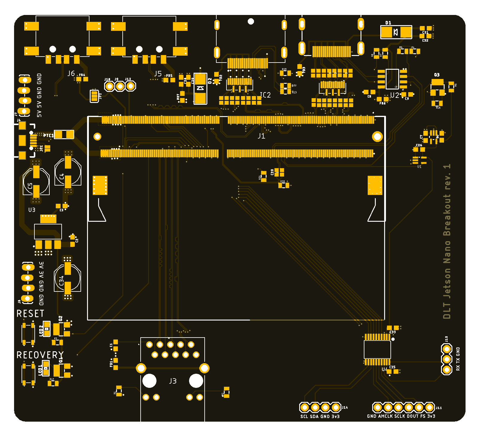
I designed a first test board with a similar goal as I had with my previous breakout for the i.MX8M. Get to know the hardware and its issues. When I'm comfortable with it I will continue with the next iteration, a first prototype that would actually be usable in my tablet form factor.
This first prototype will again just be a quick and dirty SBC. I also gave a bit more shit about HDMI and eDP, learning more about High Speed design and trying to do it "proper". I ended up rerouting the high speed stuff 4 or 5 times as I found more and more error the more I read into the topic :)
The PCB should hopefully arrive end of next week. 4 Layer impedance controlled PCB this time.
![]()
-
Soldered up and finally booting
05/01/2019 at 22:38 • 0 commentsSo the first time I soldered the new boards the SoM was still not booting.
Quite frustrating, then in a fluke accident I found out that the "ONOFF" pin is actually a pin from the PMIC and by connecting it to 5V and then letting it float again (e.g. "button press" with a piece of wire) makes it boot.
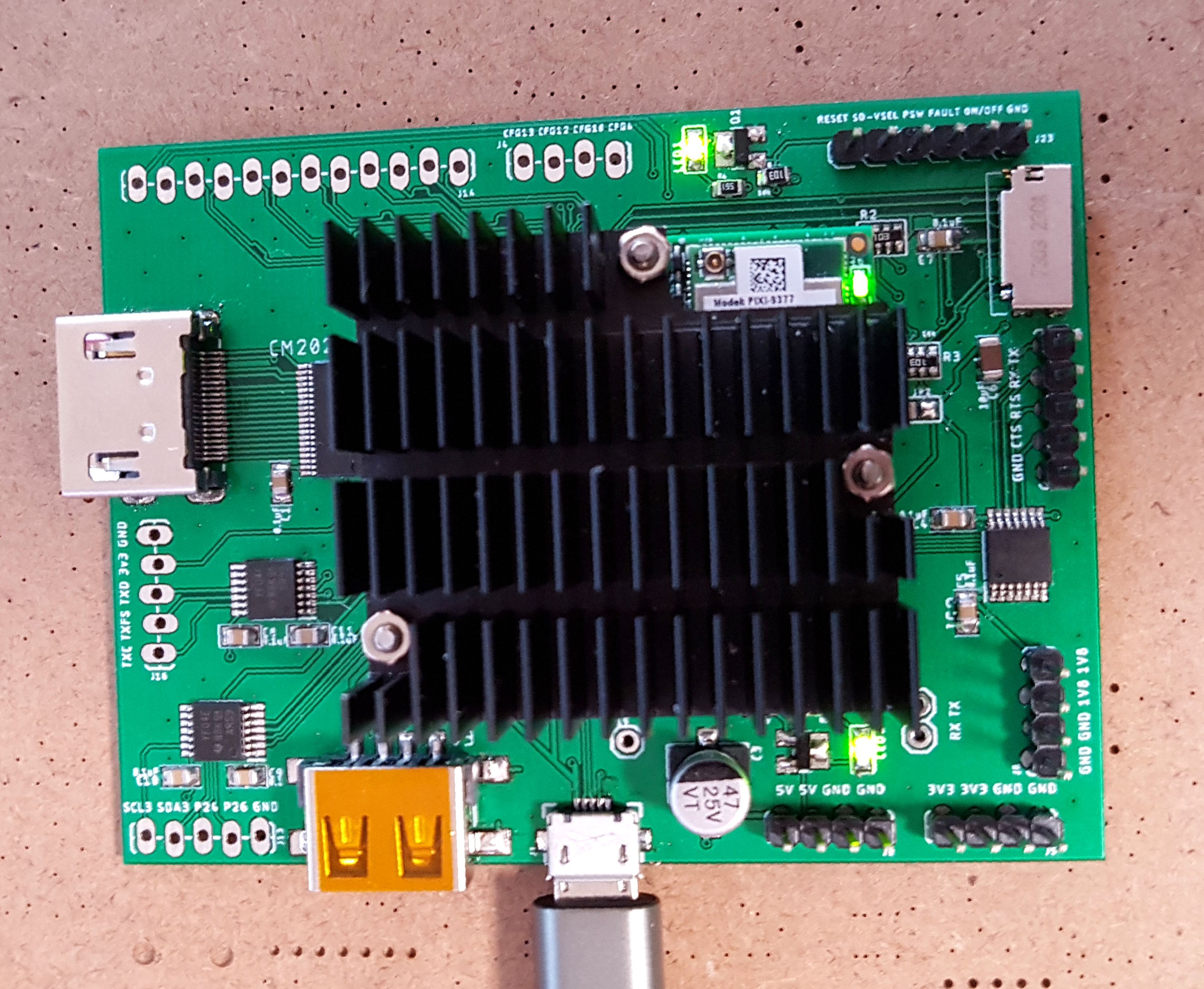
I then solderd up a second board with all components and was able to SSH into the Linux via a USB to Ethernet adapter.
So some stuff is working!
On the HDMI side I unfortunately missed the pull up resistors on the EDID lines so that seems to not work atm.Also the CPU debug serial does not come up. Not sure what the issue there is, might be an issue with the level shifter or I got the wrong UART all together.
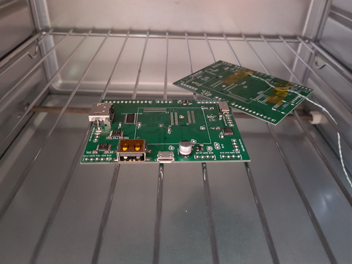
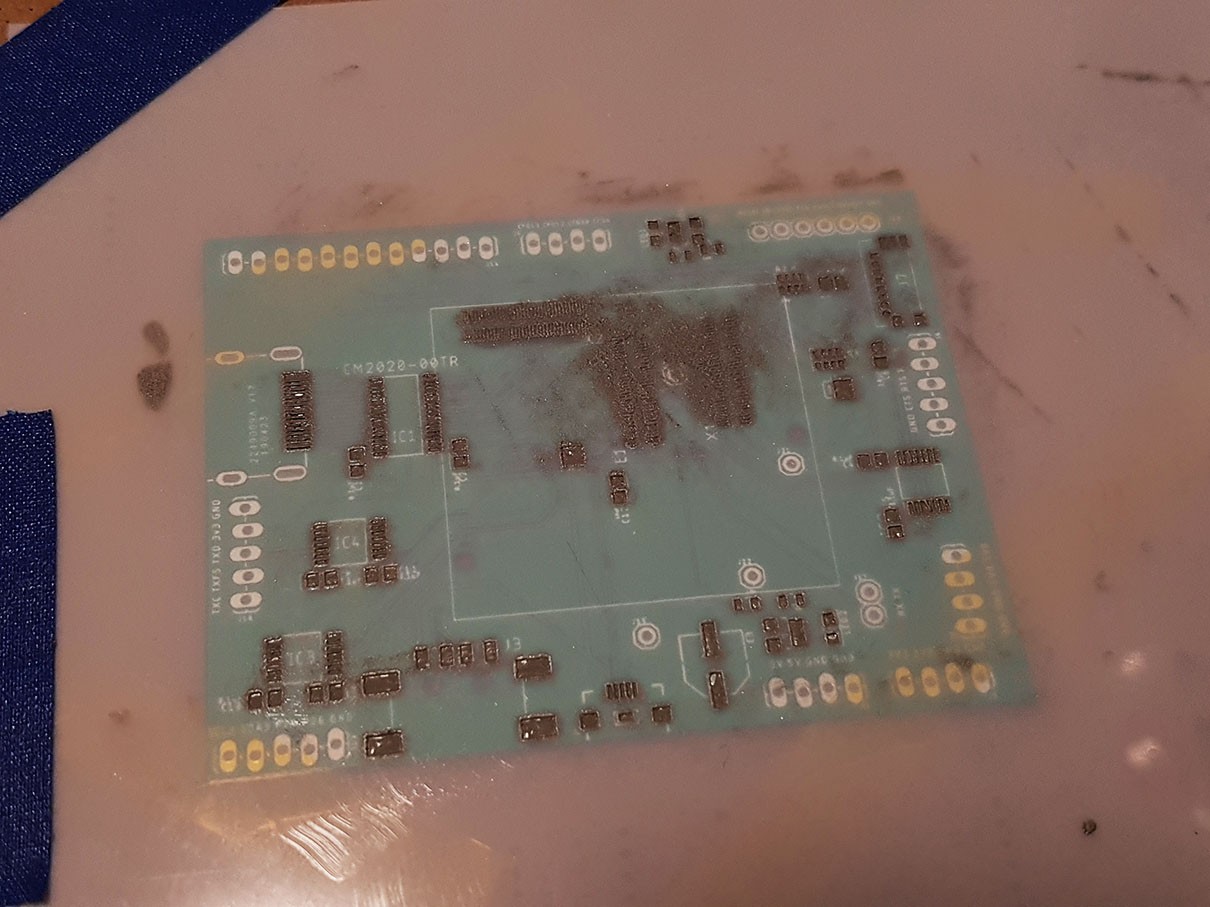
Here are some photos of the process and the finished board:
![]()
![]()
![]()
![]()
-
Ordered second prototype
04/24/2019 at 11:59 • 0 commentsI didn't get the milled PCB to work, I triple checked everything but couldn't find a root cause. Technexion is taking a look at my schematic so lets see what they have to say.
In the meantime I just went ahead with a new design as I think it probaly is just a fluke issue that I just haven't noticed yet. I ordered a PCB this time to cast out any issues arising from a missing solder mask.
My main goal is still to only get it to boot but I broke out a bunch more stuff in case I want to test more. I don't have high hopes for HDMI and DSI as I did not order a impedance controlled PCB this time and haven't taken much care to aproximate the impedance with this stackup but it will be interesting to see if it would still work, just to see how much you can abuse these high-speed busses before they completely crap out on you.
![]()
-
Unable to power up
04/19/2019 at 12:20 • 0 commentsThe past days I've been debugging my first try at a minimal carrier PCB. I milled a PCB that has power in, CPU debug serial, USB-A and HDMI.
Though the only thing I wanted to get going so far is powering the SoM and getting a connection to the CPU debug serial.
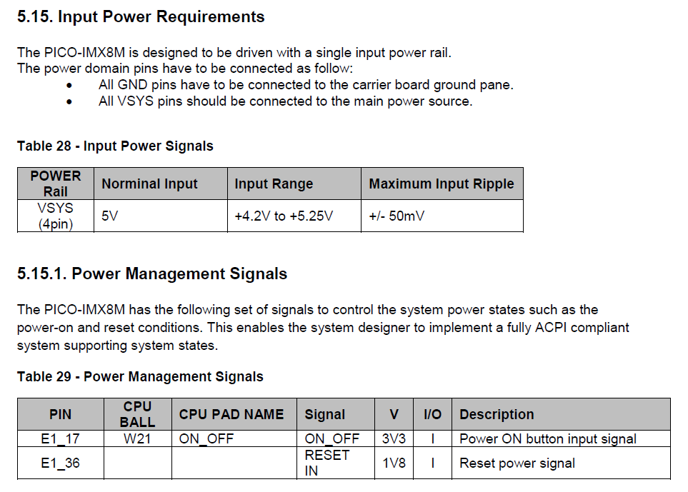
At the moment I'm struggeling to even get the SoMs PMIC to power up. I connected everything correctly according to the datasheet. All thats apparently needed is 4.2-5.2v on the VSYS pins and all GND pins connected. I continuintity up to the mating pin of the connector and they are all properly connected, so its quite puzzling why the PMIC wont even start up and produce the 3.3 and 1.8 voltages. I do get a minimal power draw of around 10mA when attaching 5V but other than that it just seems dead.
SoM is still working fine in the dev kit carrier board so I haven't fried it either.
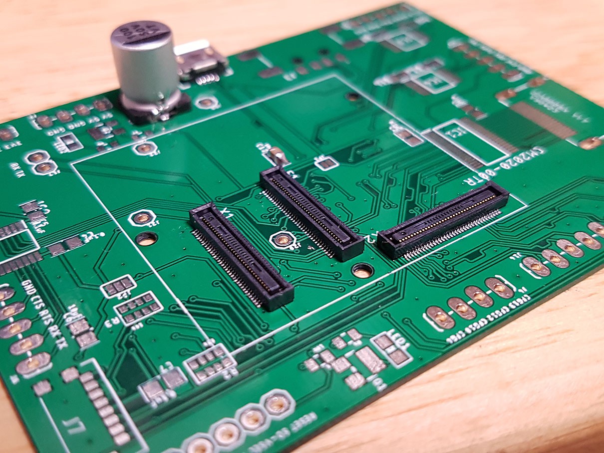
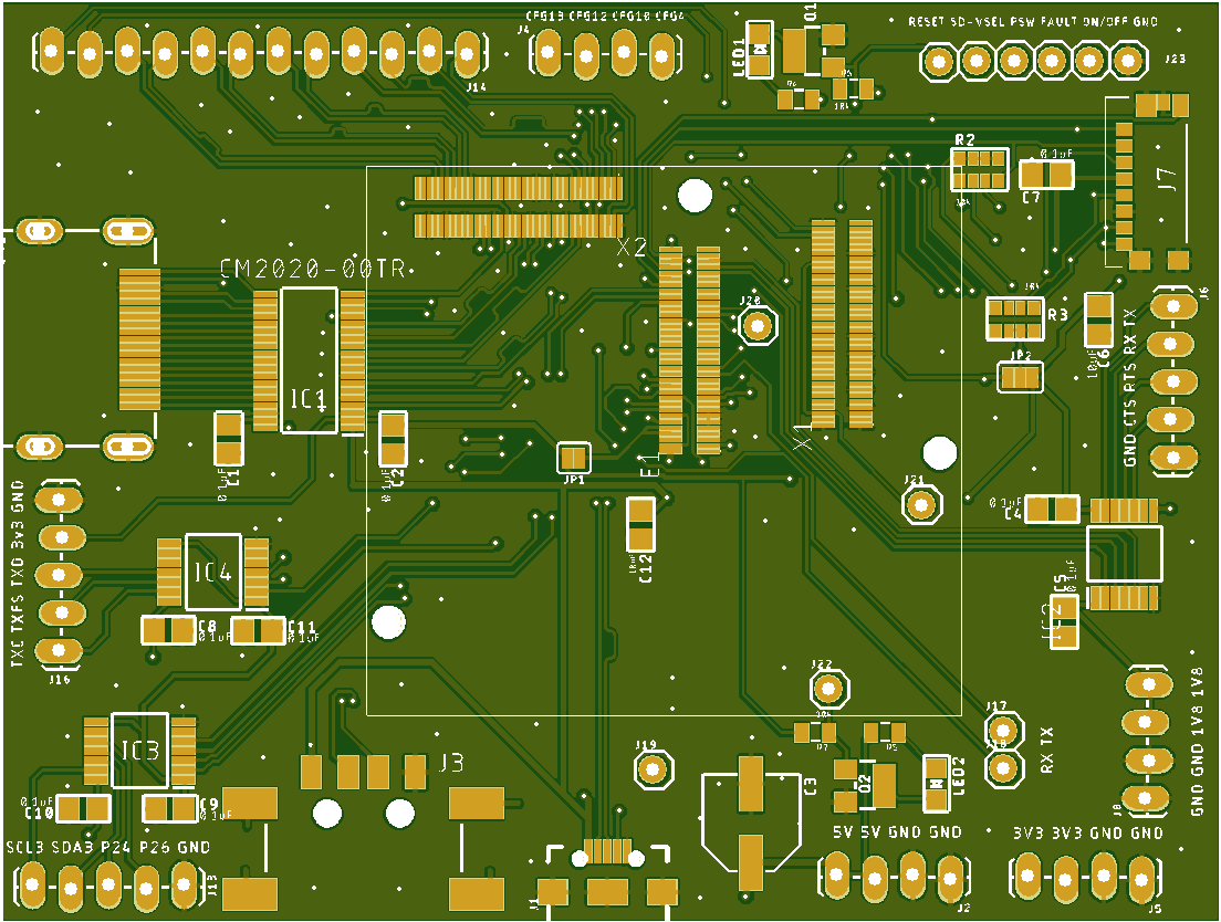
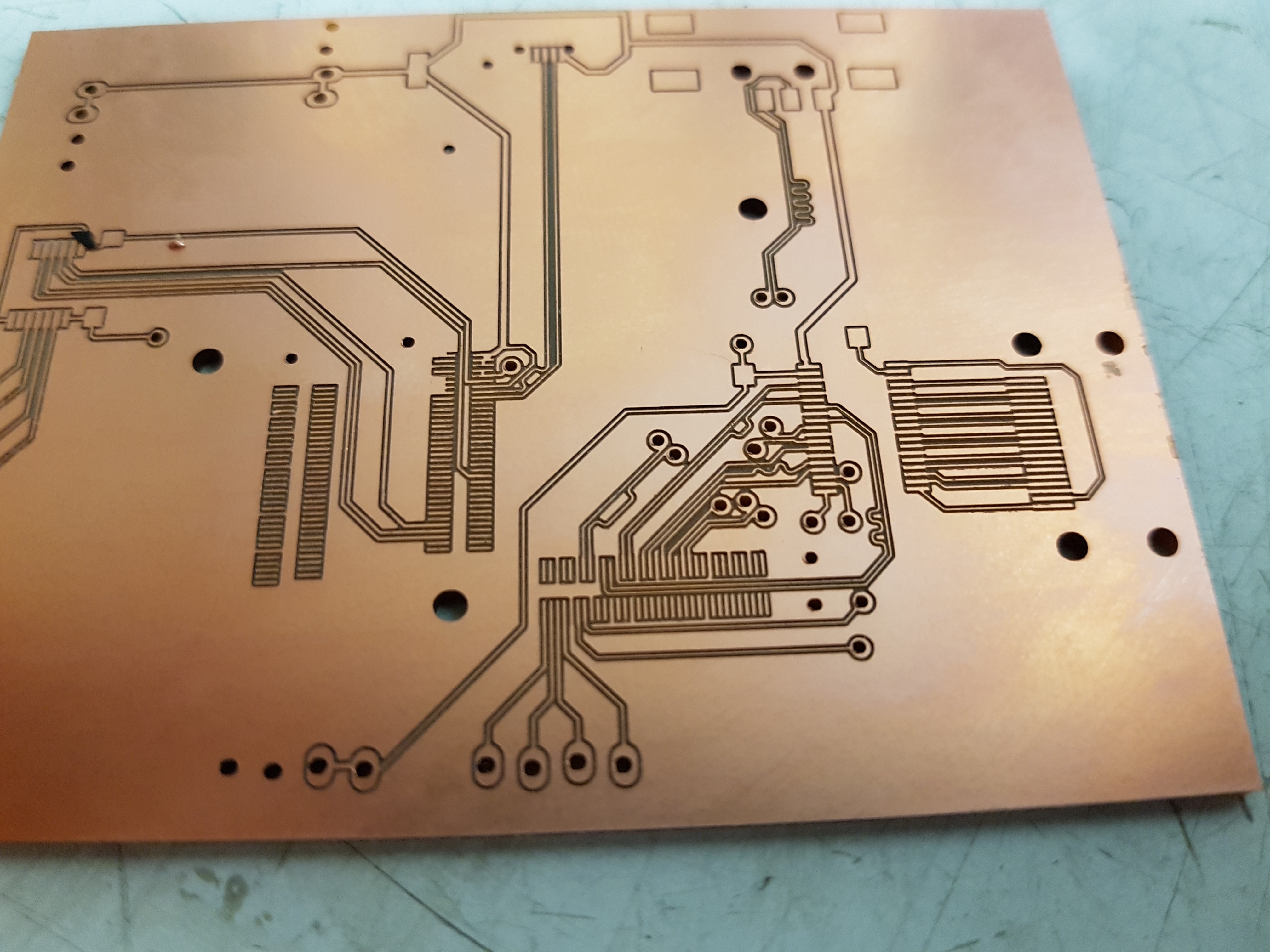
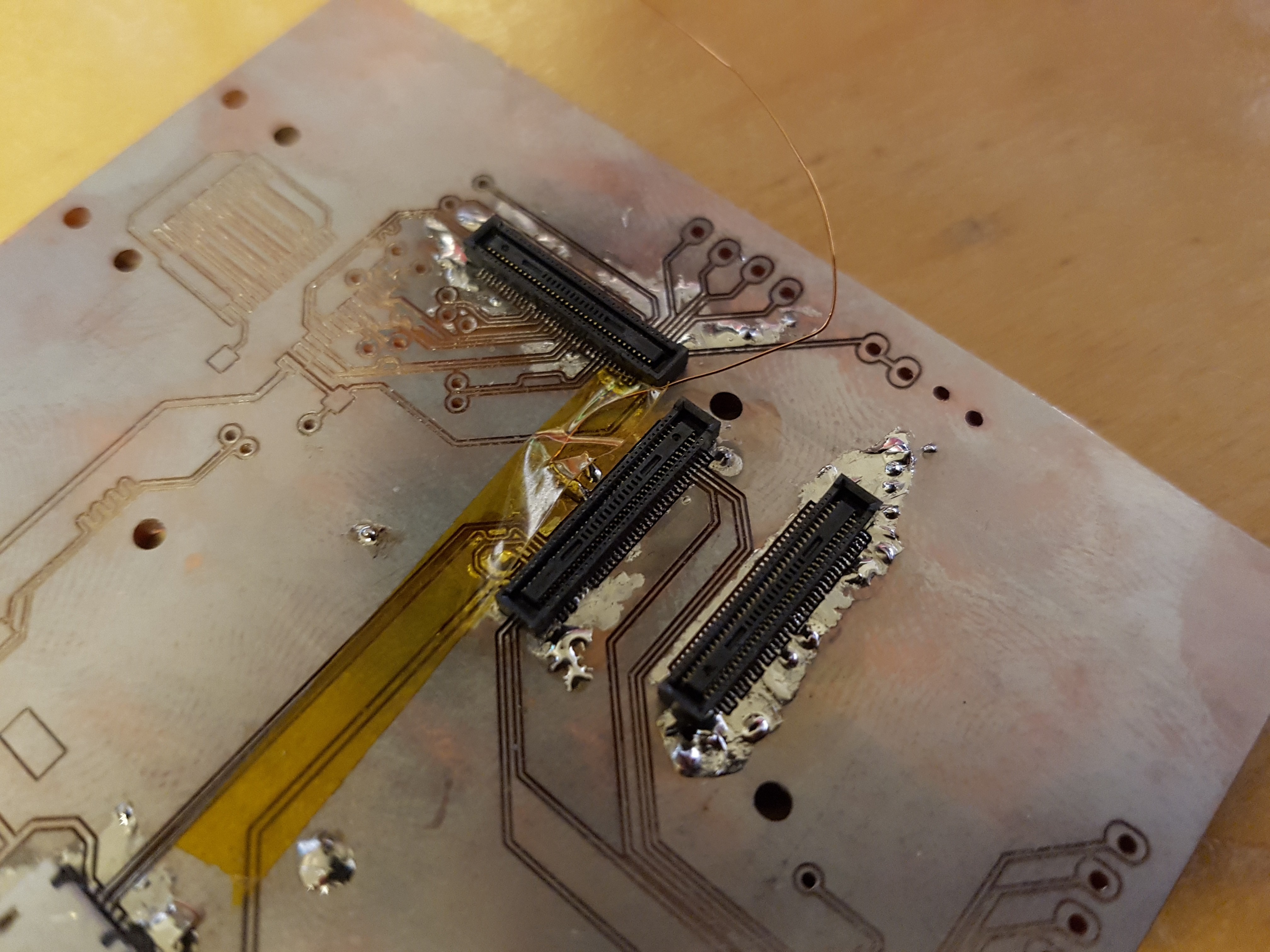
If anyone is interested here is the datasheet for the SoM: https://s3.us-east-2.amazonaws.com/technexion/documentation/pico-imx8m-rev099.pdfA pic of the milled carrier board (yes the connectors are shit to solder, they have no alignment pins)
![]()
![]()
Here the excerpt from the datasheet
-
Dev-kit arrived and working
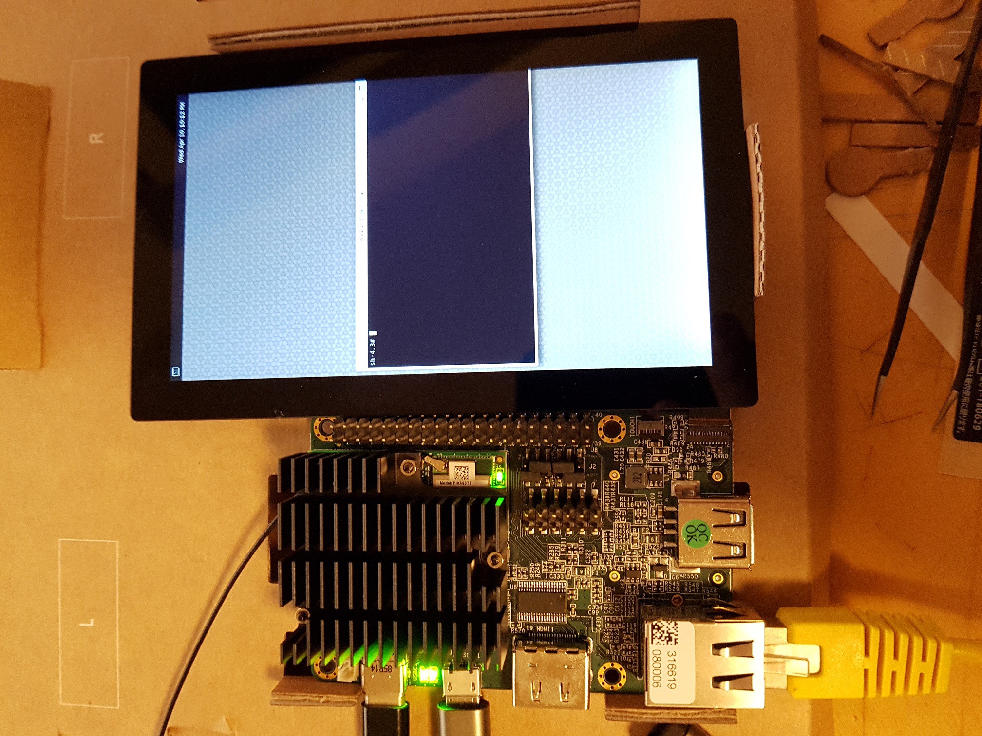
04/11/2019 at 22:07 • 0 commentsJust a quick update. I got the dev-kit in the mail yesterday, I booted it up with the touch screen attached that it came with. Was all working fine so today I started working on making a first break out which I will mill tomorrow to do a first test fit with the SOM connector. As there 3x70 pin connectors the positioning of them in relation to each other is very important.
Technically it should fit perfectly as I worked according to Technexion specs but lets see how it goes after they are soldered to a board.
![]()
-
What this is going to be and what not
04/09/2019 at 21:43 • 0 commentsAs a lot of people seem to get very excited about this project (which is fantastic). I want to address some thing to manage expectations.
What I want to build here is a basic platform for a tablet computing device. I will not write fancy software to make this a typical end consumer tablet so you can have an awesome Linux tablet in your backpack to check your Twitter feed and do your daily work with it. This is actually really hard and the main reason why no one with commercial interest has done this yet.
All I want to make is a hardware foundation which of course also means making sure the hardware has good driver support. After that, it is up to you what you do with this.
Compile your own version of Android for it and use it as a consumer tablet? Sure! I don't think the hardware will ever perform as well as any commercial tablet in the same price range but if that doesn't matter to you because it can solve specific issues for you that is great!
Want to add a weird sensor to the tablet and run a minimal Linux distro on it with a single application x11 instance to run a single app 24/7 on it? Great! This what I'm making this for, giving other developers a starting point to do cool stuff that is not possible with other devices :)
And of course there is always the possibility that I will fail miserably. I do have a fair bit of confidence that I can pull it off but who knows what horrible things await me in the ultra high-speed realm of USB 3.0 and dual channel MIPI :)
Over the years I read up quite a bit on high-speed signal routing and managing impedance so I hope I got enough of a basic understanding to make this work. If high-speed signal routing is a topic you are experienced in I would very much like to hear from you and ask you some questions!
This one big reason why I want do make this open source, so that when there is some grunt work done, other people get inspired to chime in and improve on this together with me.
DLT one - A Damn Linux Tablet!
Modular Open Source Hardware Tablet that is easy to hack and can run a standard Desktop Linux Distribution (or Android)
 timonsku