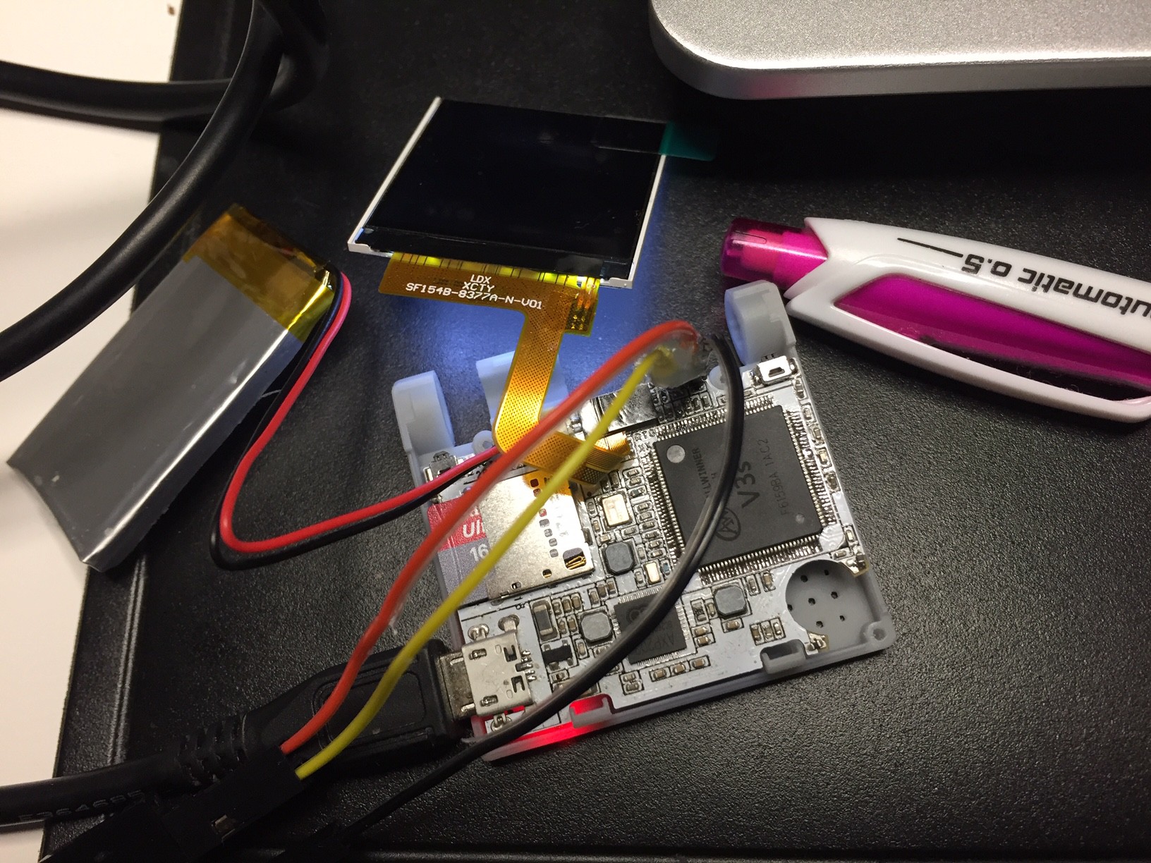
The first prototype only had a solder bridge between 2 SD Card connector pins, preventing it to boot from the card. It took us a few days to figure it out.
Here is the second prototype, which caused us more headaches: one of the power inductors was broken, some solder joints were not good, and the big V3s CPU chip (LQFP with 128 pin) was offset by almost one pin. We had to remove it completely and solder a brand new one in place. First, it didn't work, but we eventually had the board booting after pouring solder paste from below the chip to have its central die pad connected to GND.
How fun is hardware debugging!
 Squonk42
Discussions
Become a Hackaday.io Member
Create an account to leave a comment. Already have an account? Log In.